Sign-off timing analysis is a vital step in the electronic design automation process. This analysis validates a design's timing and ensures that it meets the performance specifications. It involves simulating the design at various levels of abstraction in order to test its timing behaviour and identify and correct any potential timing violations. Typically, the analysis is performed at the end of the design flow, just before the design is sent to fabrication. This ensures that the final product meets the desired performance specifications. The analysis of sign-off timing is crucial in ensuring the reliability and functionality of electronic devices and systems.
STA is a technique for improving a design's timing performance.
- Features - static, exhaustive, functionality, conservative
- STA is only used for Synchronous Design
- Netlist
- Constraint file or Synopsys Design Constraint (SDC)
- logic libraries
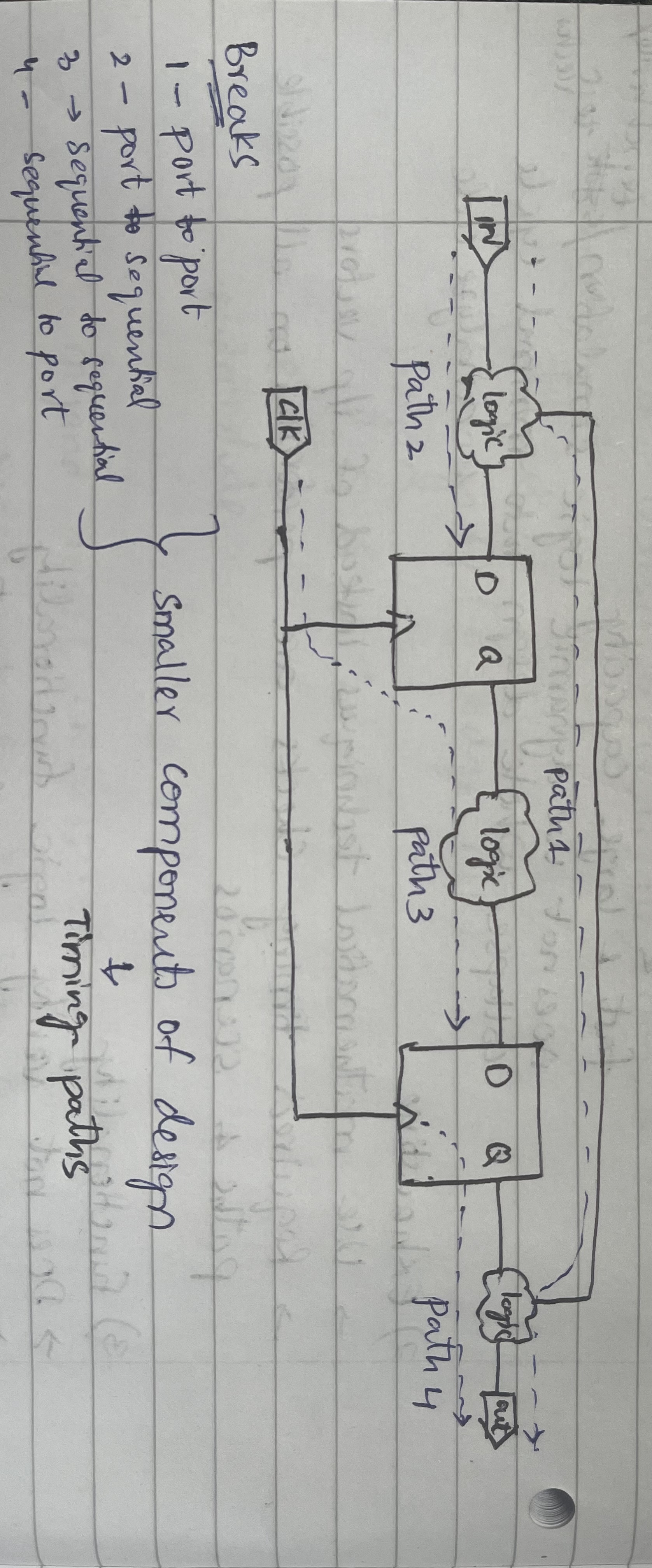
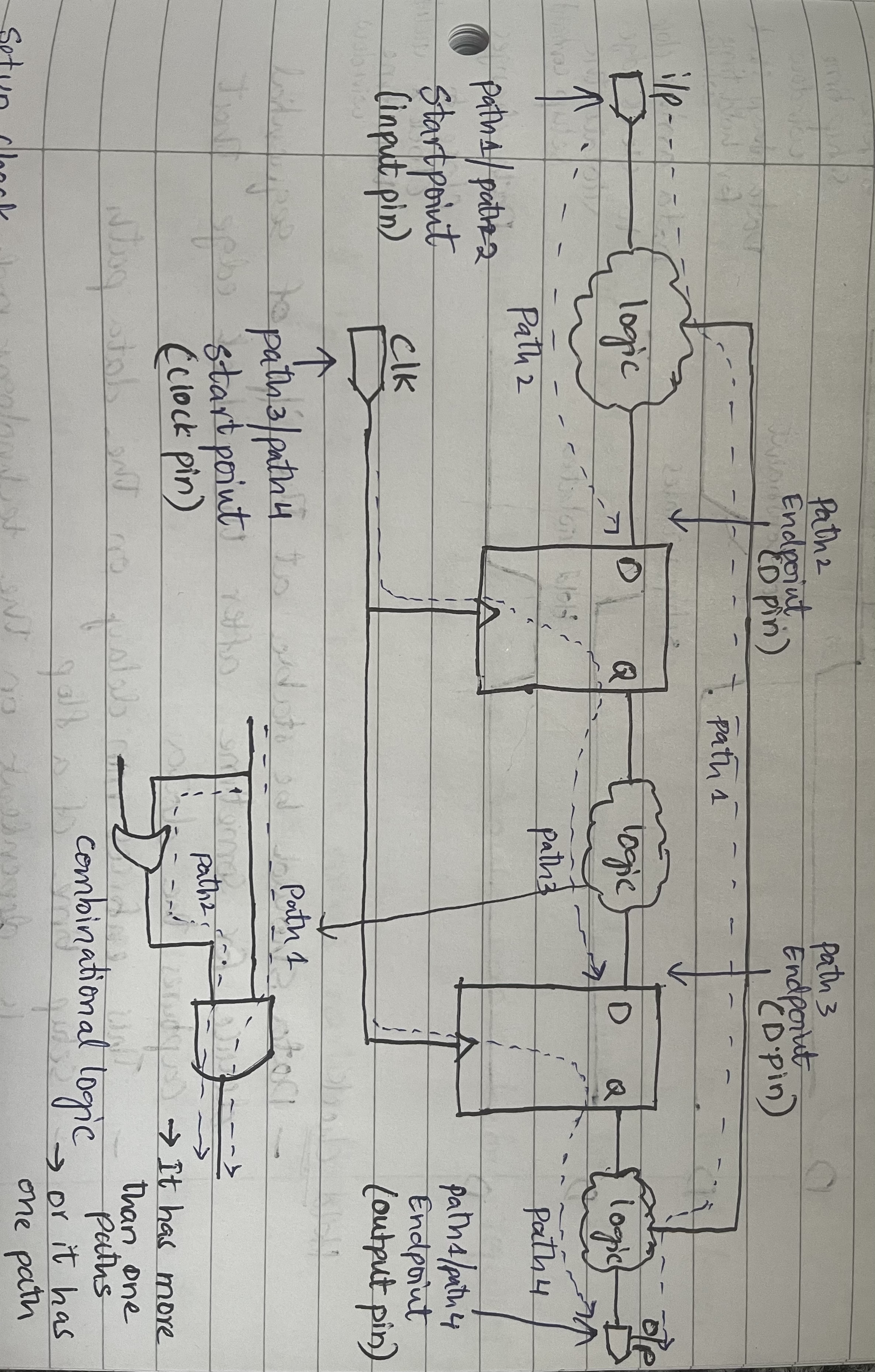
To perform design analysis, STA divides the logic design into ports and sequential elements.
-
Startpoint
- where the data is launched by the clock edge
- where the data must be available at a specific time
- input ports or register clock pin
-
Endpoint
- where the data is captured by clock edge
- where the data must be available at a specific time
- output ports or register data pin
-
Combinational Logic
- Elements that have no memory element or internal state
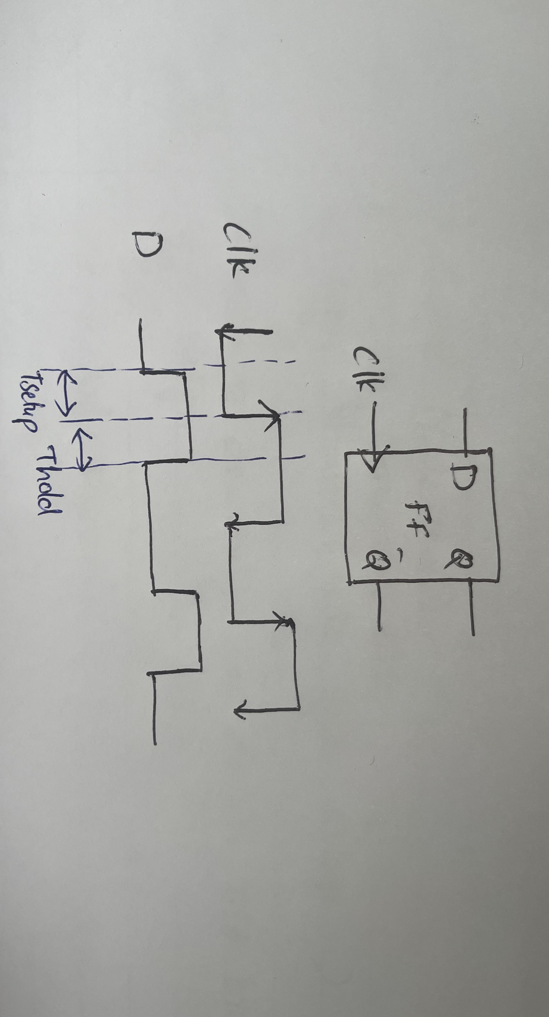
SETUP
- The data should be stable at the input of sequential device for sometime before the clock edge that captures the data.
- This sets the maximum data path delay.
HOLD
- The data should be stable at the input of sequential device for sometime before the clock edge that caputers the data.
- This sets the manimum data path delay.
** For setup and hold checks of a flop is dependent on the technology node and value is available in logic libraries.
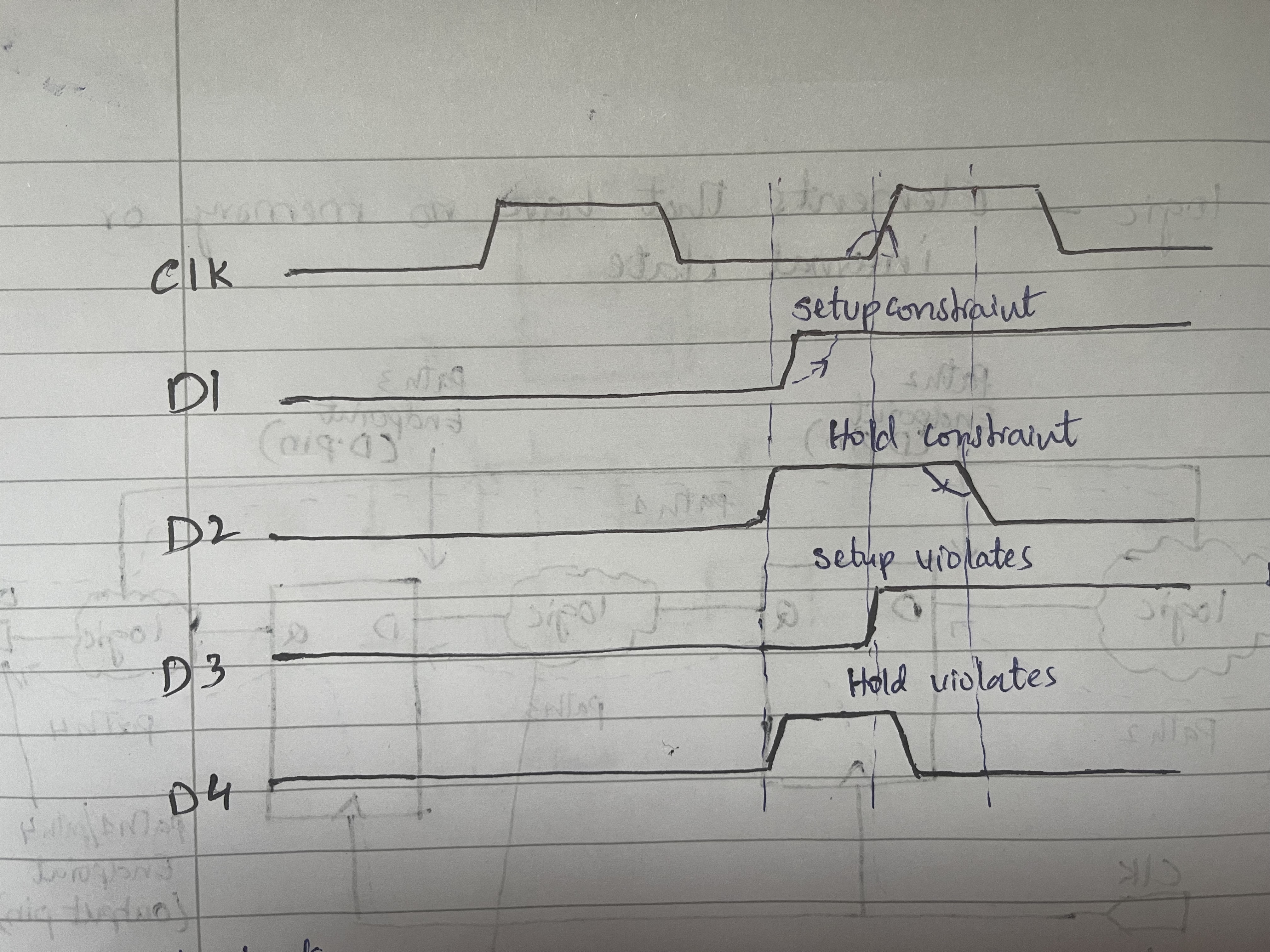
To understand the setup and hold checks, DATA (d) is denoted as D1, D2, D3, D4 in the waveform above.
D1 - Data arrives before the setup time window
D2 - Data stays stable for hold for hold time window
D3 - Data arrives close to clock edge violates the setup constraint
D4 - Data arrives close to clock edge violates the hold time constraint
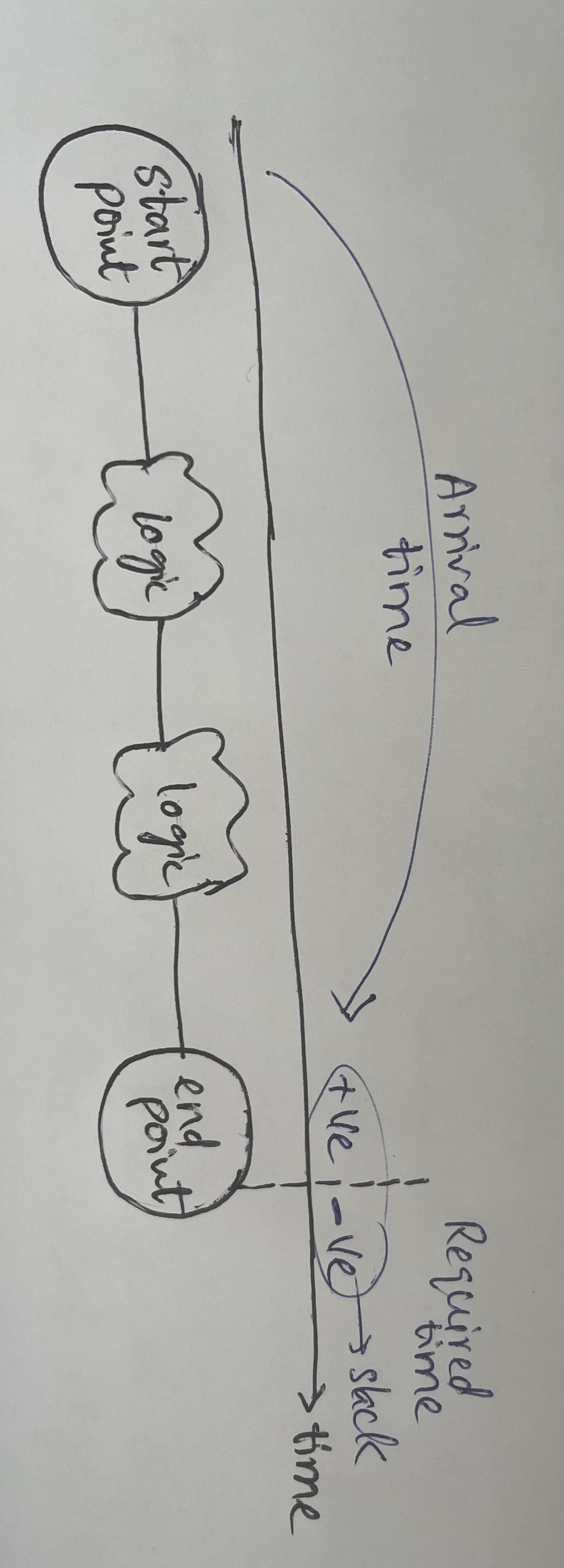
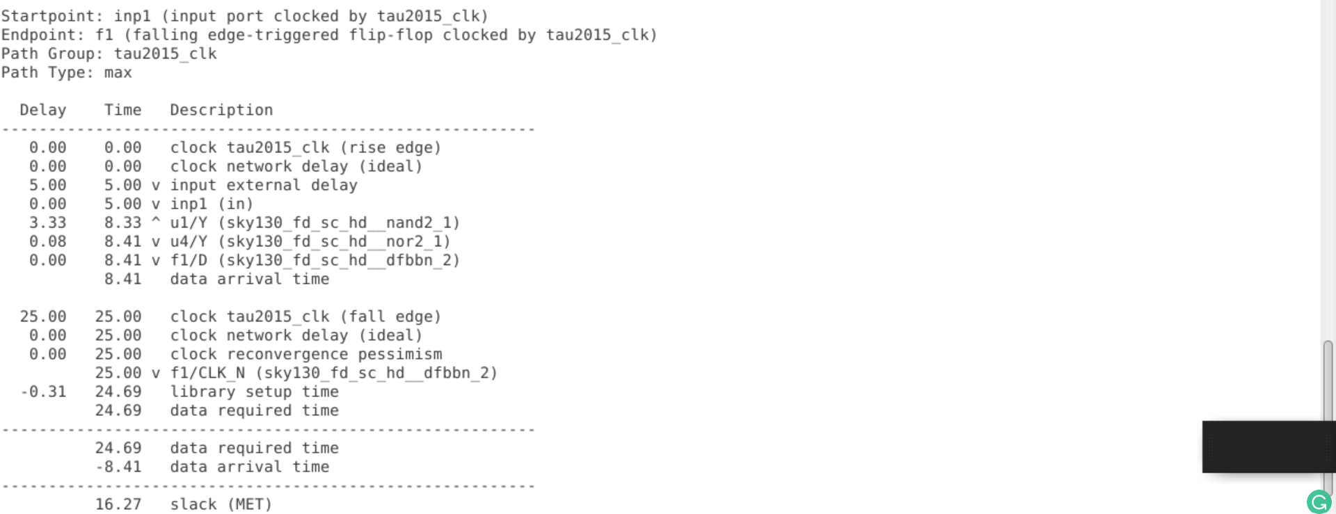
Arrival Time - Time it takes the signal to travel from startpoint to endpoint.
Required Time - The signal should arrive before the specified time.
Slack - The difference between the required arrival time of a signal and the actual arrival time of the signal at the destination
- slack is +ve - when data arrives earlier then required time
- slack is -ve - when data arrives later then the required time
setup slack
setup slack= Data Required Time- Data Arrival Time
hold slack
hold slack= Data Arrival Time- Data Required Time
- Constarints for timing - specify parameters affecting operational frequency of the design
create_clock create_generated_clock set_clock_groups set_clock_transition set_timing_derate - Constraints for area and power - specify restrictions about the area and power
   set_max_area
   set_max_dynamic_power
- Constaints for design rules - requirements of the target technology
    set_max_capacitance
    set_min_capacitance
    set_max_transition
    set_max_fanout
- constarints for interfaces - assumptions on the design boundary
set_driving_cell
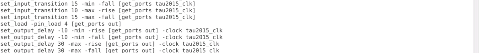
set_input_delay
set_output_delay
set_load
- Contarints for specific modes and configurations - assumptions on the values allowed
   set_case_analysis
   set_logic_dc
   set_logic_one
   set_logic_zero
- Exceptions to design constraints - relax the requirements set by the other commands or default sta tool analysis
   set_false_path
   set_multicycle_path
   set_max_delay
   set_min_delay
   set_disable_timing
clocks are specified in timing constraints using command
create_clock -period 10 -waveform {2 4} {C1 Ck} -name
Where
create_clock - It specifies primary source input ports of the design
-period 10 - period of the clock (10 units)
-waveform {2, 4} - period when it rises and falls
{C1 Ck} - attaching  the clocks in the design
-name - name of the clock
clocks which are created inside the design using commands
create_generated_clock -divide_by 2 -source C1 -master_clock CLK1 {GC2 GC1}

## Divide by (edges have odd number of elements - rise at 1, fall at 5, rise at 7)
create_generated_clock -edges{1 5 7} -name DIV3A -source SYSCLK {GC}

## To generate pulses
create_geerated_clock -name pulse -source CLK1 -edges{1 1 3} -edge_shift{0 2 0}{pulsegen}
 set_input_delay
 set_output_delay
set_port_fanout_number - number of pins in fanout
set_fanout_load - load in multiple of standard cell/buffer
set_load - load in terms of capacitance value
set_drive - specifies resistance value
set-driving_cell - specifies cell driving port
set_input_transition - specifiestransition value
- OpenSTA is a gate level static timing verifier. It can be used as a standalone executable to verify the timing of a design using standard file formats.
- Verilog netlist
- Liberty library
- SDC timing constraints
- SDF delay annotation
- SPEF parasitics
- OpenSTA is designed to be easily bolted on to other tools as a timing engine. Using a network adapter, OpenSTA can access the host netlist data structures without duplicating them.
- Query-based incremental update of delays, arrival, and required times
- Simulator for propagating constants from constraints and netlist tie high/low
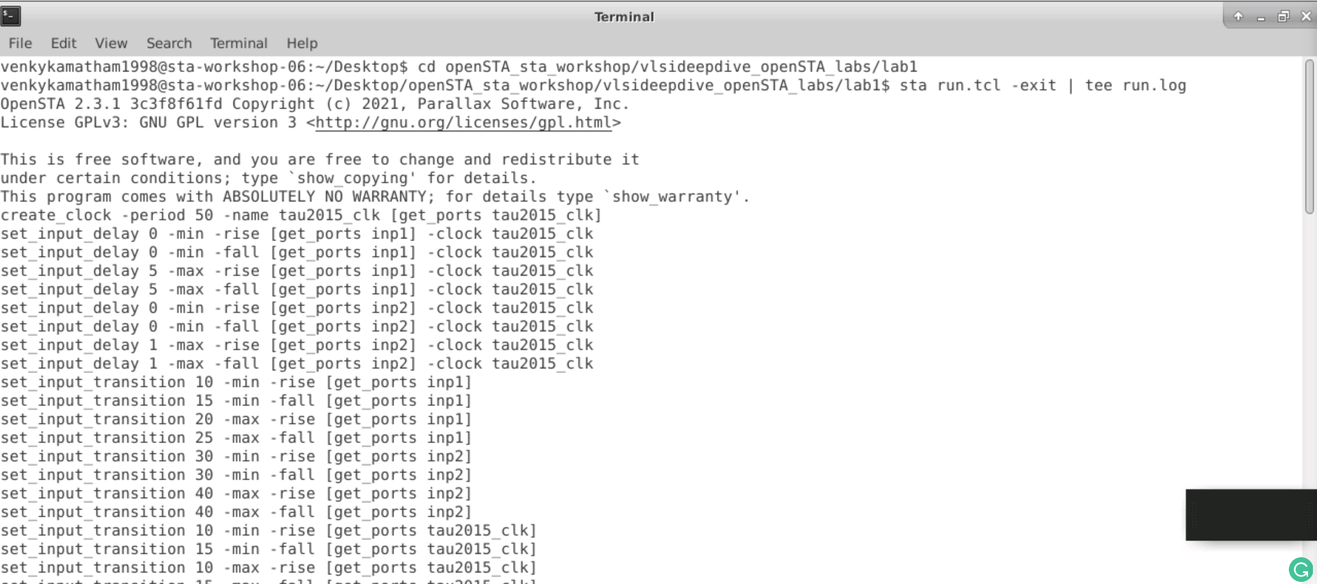
git clone https://github.com/vikkisachdeva/openSTA_sta_workshop
cd openSTA_sta_workshop/vlsideepdive_openSTA_labs/lab1
ls
leafpad simple.v

leafpad sky130_fd_sc_hd__tt_025C_1v80.lib
leafpad  simple.sdc
leafpad run.tcl
To run sta
sta run.tcl -exit | tee run.log
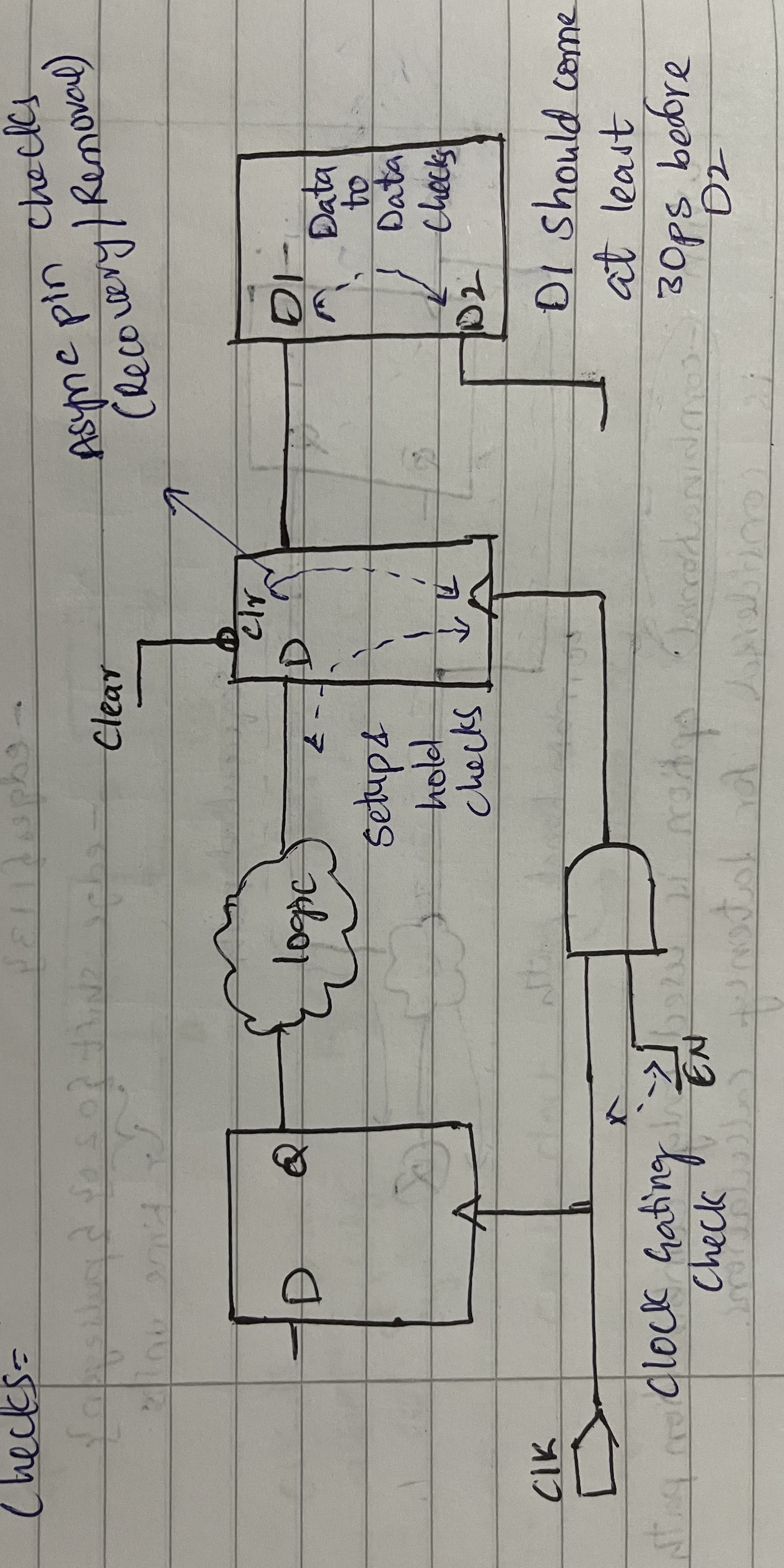
STA will perform additional checks in addition to the setup and hold checks.
- Clock gating check
- Asynchronous pin checks
- Data to data checks
-
Slew/Transition analysis
- Rise Slew - Time taken by a signal when it rises from 70% to 30% of vdd
- Fall Slew - Time taken by a signal when it falls from 70% to 30% of vdd
-
Load analysis
It is the process of evaluating a design's timing by analyzing the effects of load capacitance on signal propagation.
- minimum and maximum capacitance on ports and nets
- fanout load on ports and output pins
- Clock skew analysis
The Difference in delays of the clock at different points in the path.
- skew +ve - Capture clock has more delay than launch
- skew -ve - Launch clock has more delay than capture
- pulse width checks
Pulse width checks are used to ensure that a sequential element's output waveform meets a minimum or maximum width requirement.
- The flop-based design data is launched and captured on the edges, and regardless of the delay, it must be stable for one clock period.
- It allows more flexibility in timing
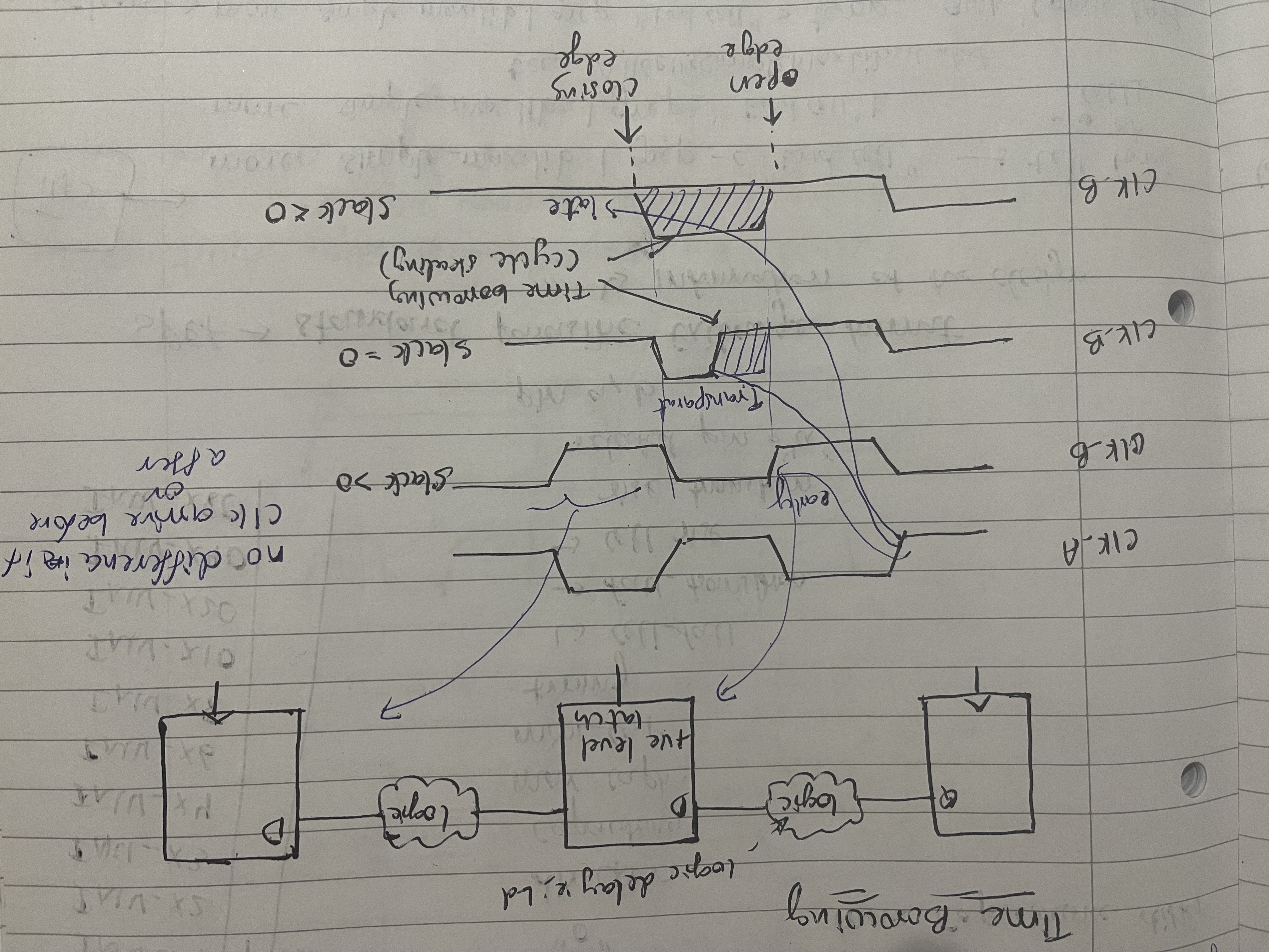
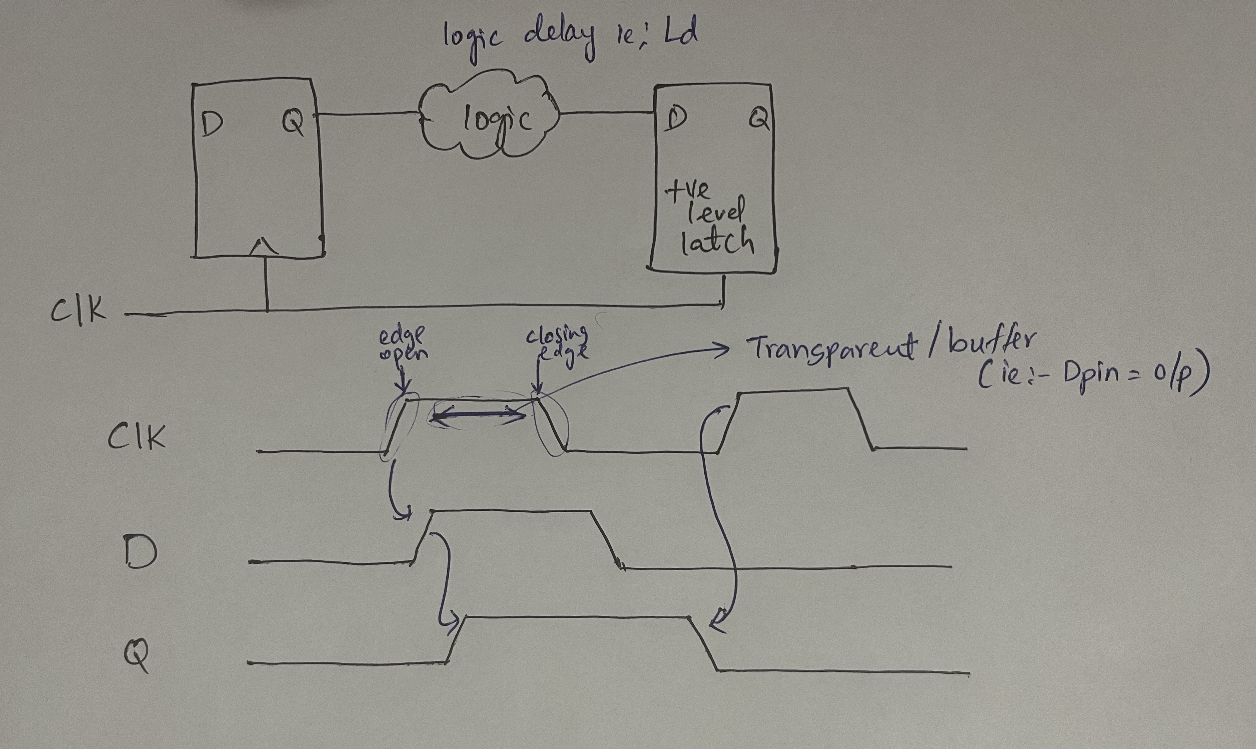
Time borrowing is a technique for adjusting the timing of two distinct paths. It is possible to accomplish this by borrowing or lending some delay from/to a neighbouring path. A latch is placed in the path that has a timing violation. This latch acts as a buffer, delaying the signal and allowing the previous stage to complete its operation. The latch's output is then transferred to the next stage.
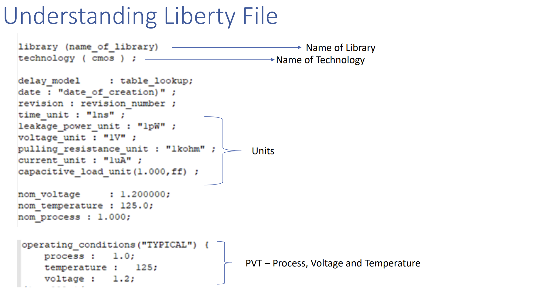
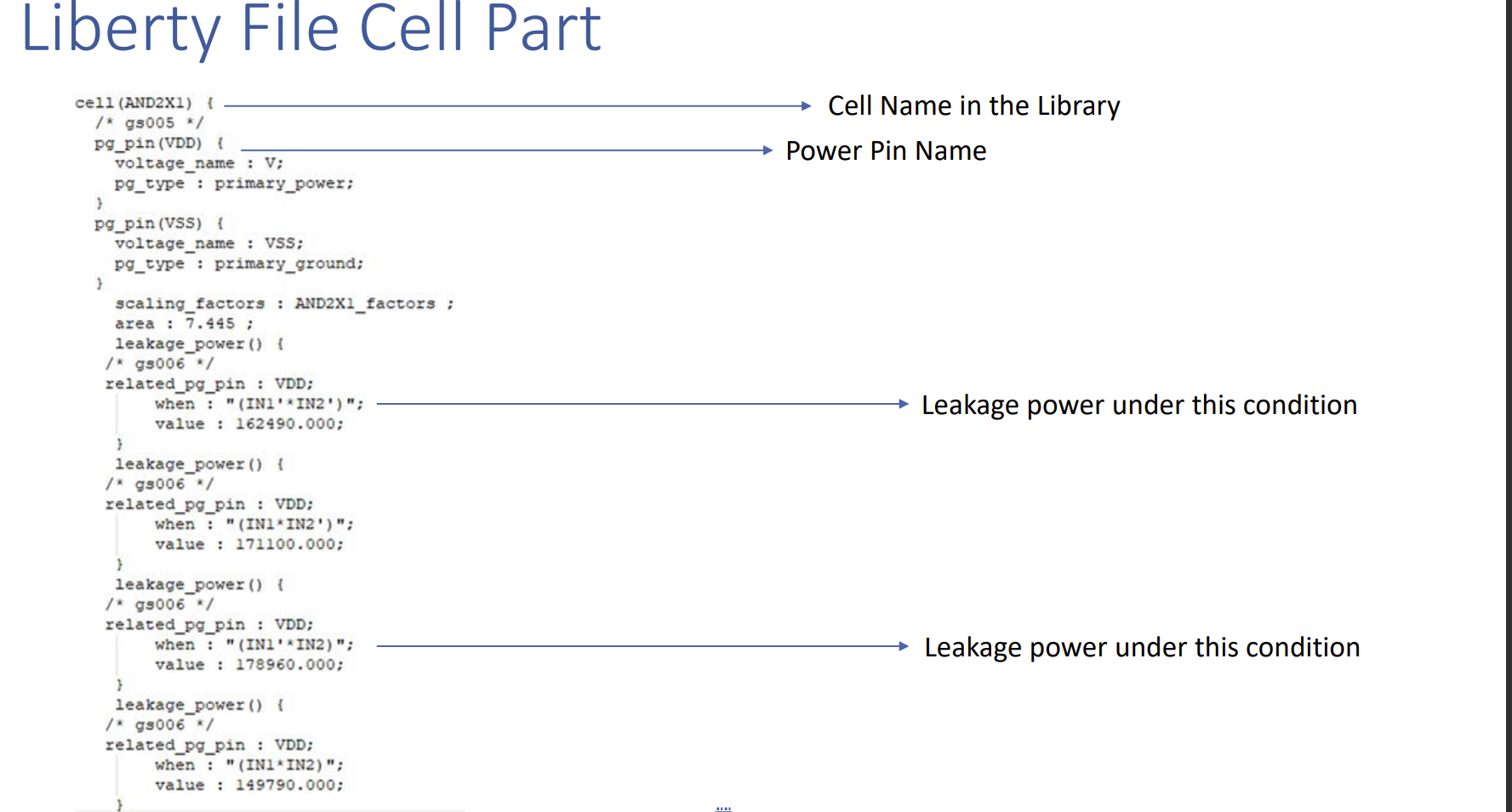
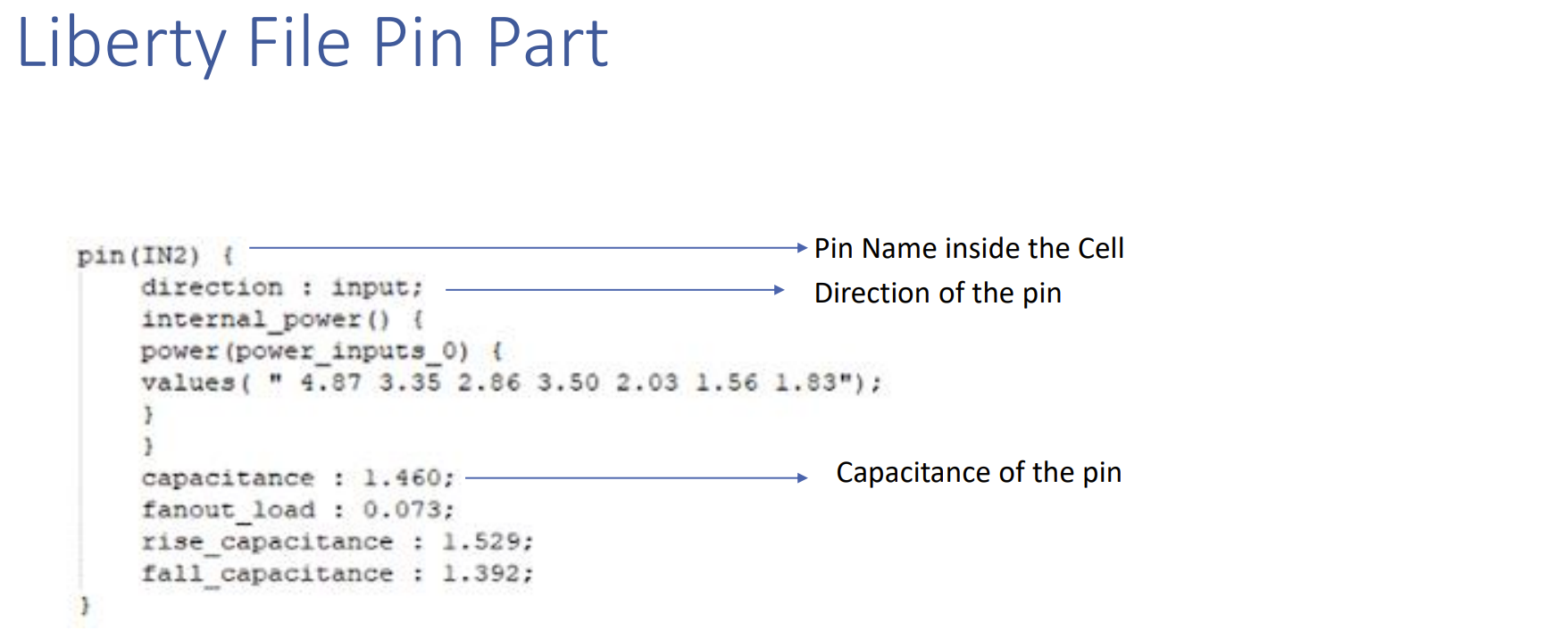
Liberity File The.lib file is an ASCII representation of the timing and power parameters associated with any cell in a specific semiconductor technology.
- The .lib file contains timing models and data to calculate
- I/O delay paths
- Timing check values
- Interconnect delays
Lab
cd lab2
leafpad simple_min.lib
leafpad simple_max.lib

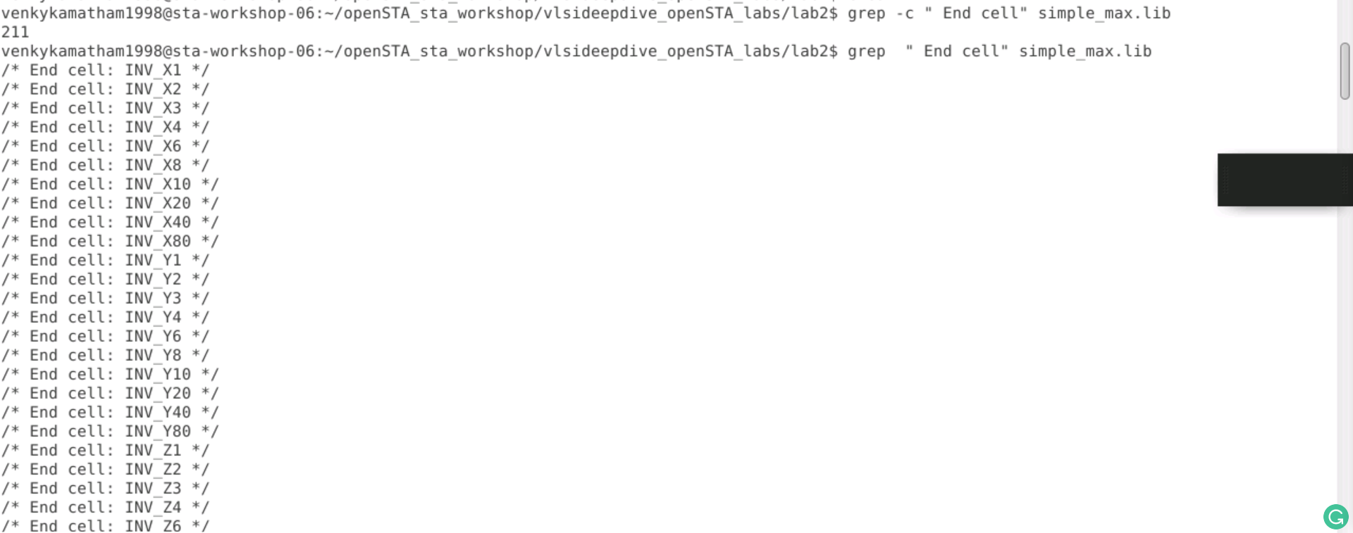
To find all of the cells in simple max.lib
# total no of cells
grep -c " End cell" simple_max.lib
# cells
grep -c " End cell" simple_max.lib
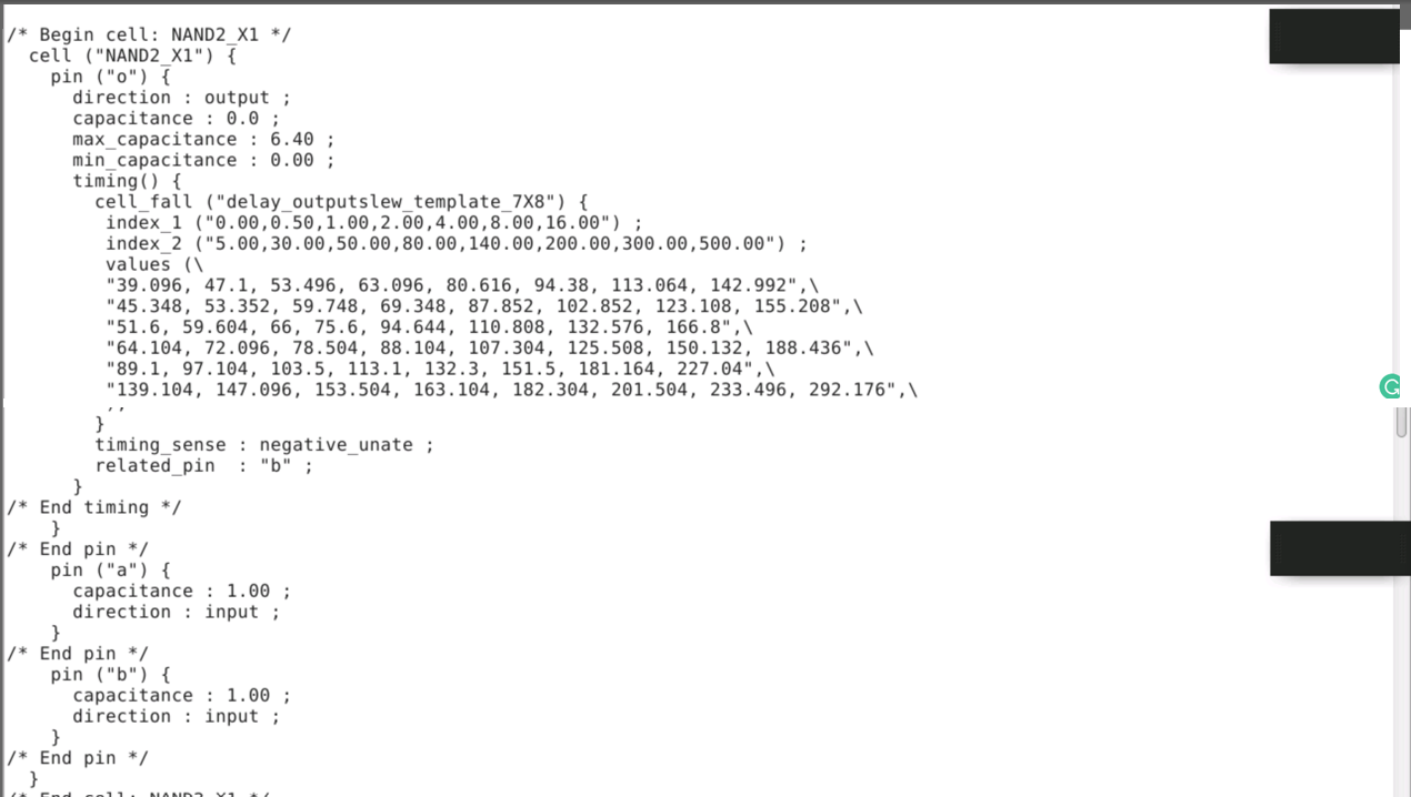
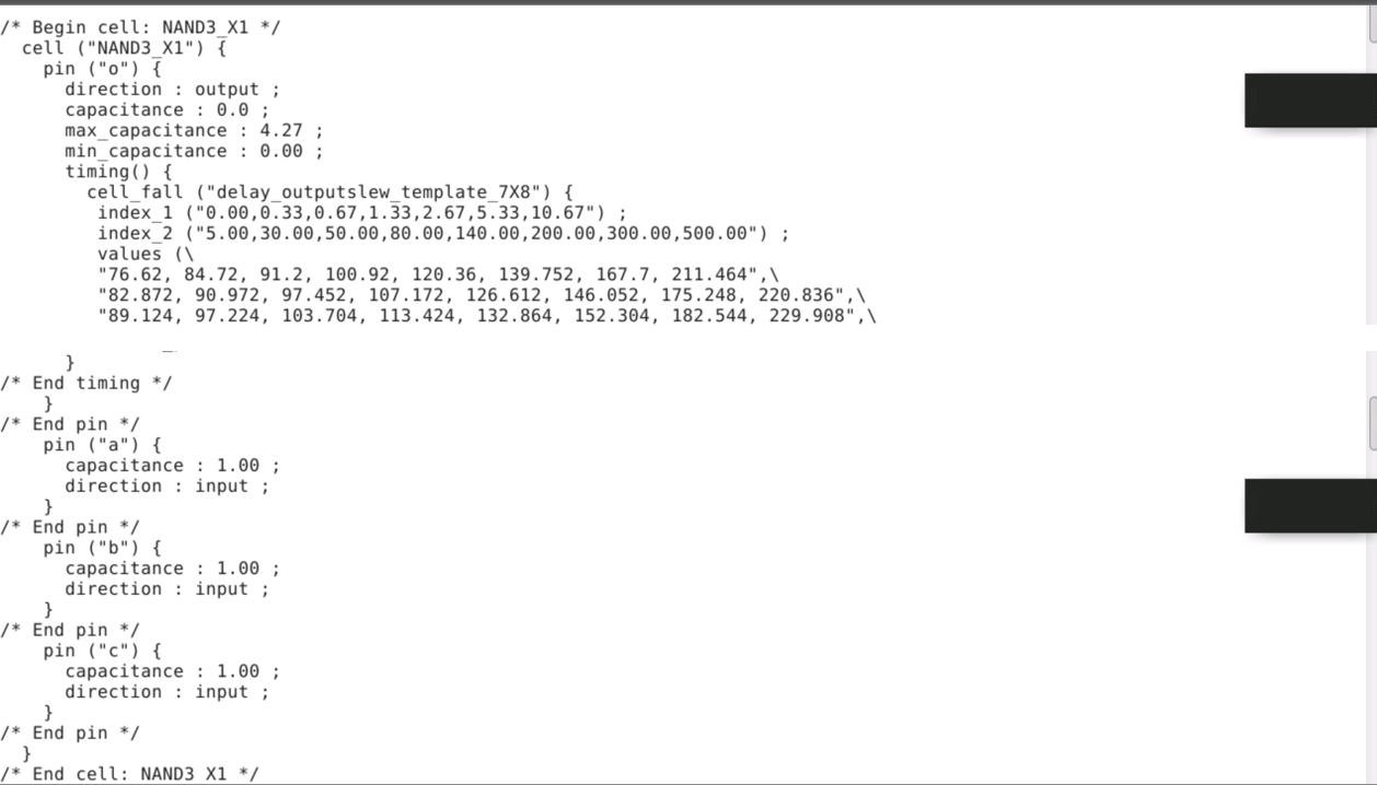
The pins of the cell NAND2_X1 in simple_max.lib

The difference between NAND2_X1 and NAND3_X1
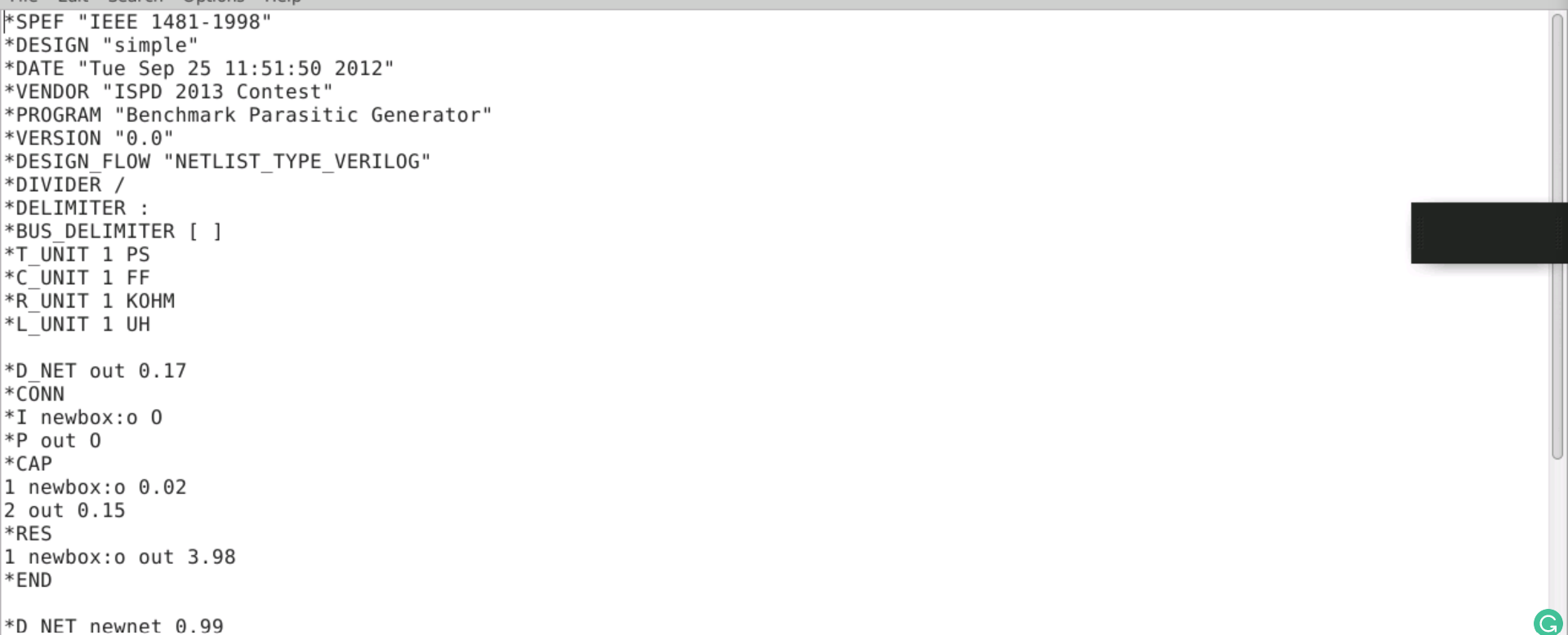
A SPEF (Standard Parasitic Exchange Format) file describes the design's parasitic information.
- Users would never manually create this file.
- It is generated automatically by the tool.
- It is primarily used to transfer parasitic data from one tool to another.
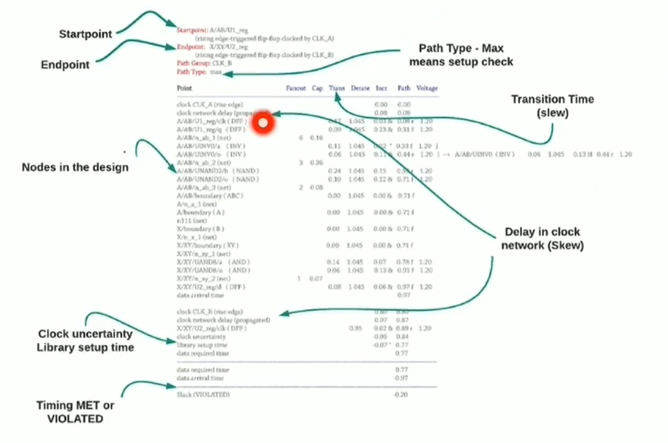
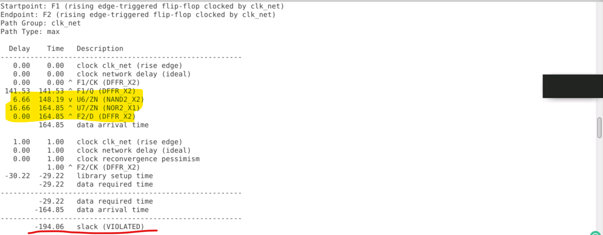
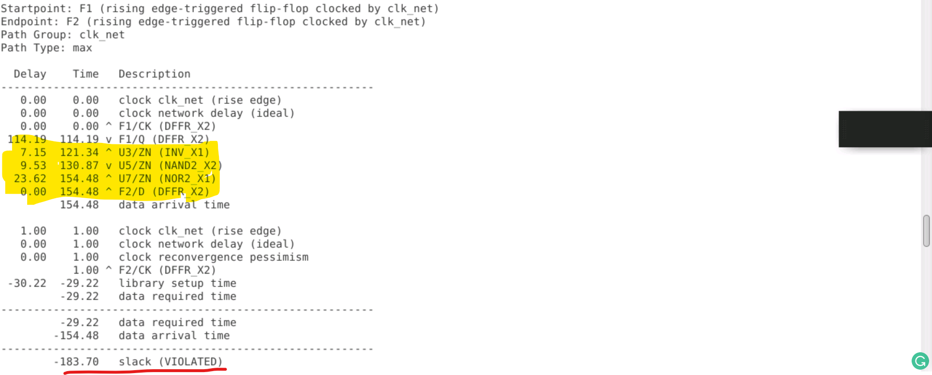
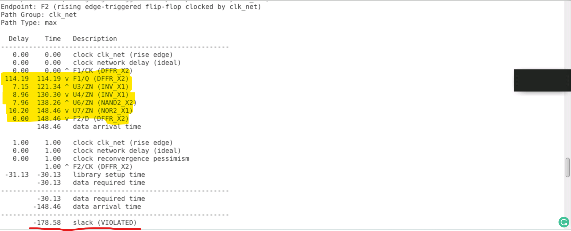
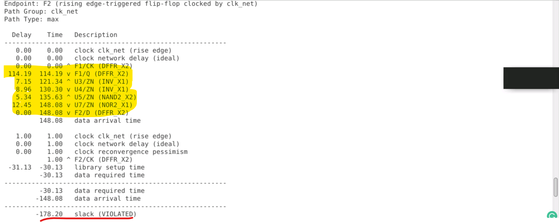
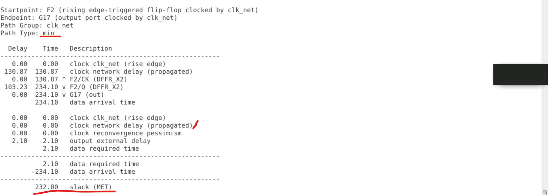
add report_timing –num_paths 5 in tcl file
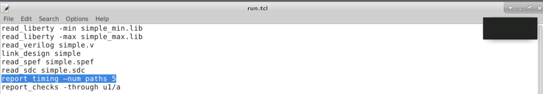
run sta
sta run.tcl | tee run.log

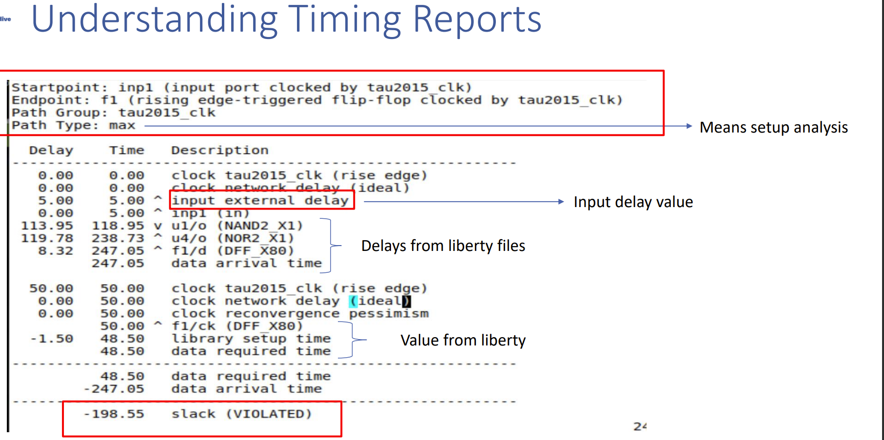
understanding timing report
- If there are multiple clocks with different frequencies, a setup check is performed by expanding the clock to a common base period and identifying the most restrictive setup.
- There are two rules for the hold check
- The data launched by the current setup launch edge cannot be captured by the previous capture edge.
- The Data launched by the following launch edge must not be captured by the current setup capture edge.
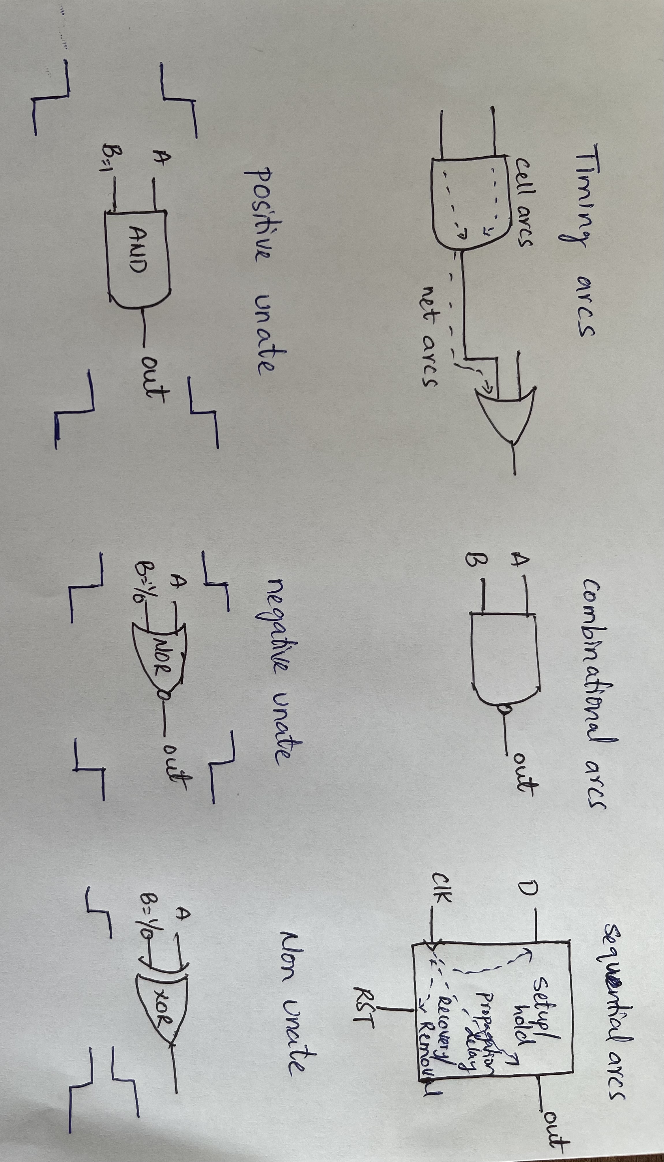
- Timing arcs
- Timing arcs are classified into two types:
- cell arcs - input to output connected cells
- net arcs - connection one cell to another
- Combinational arcs
- It is a logical path or a signal path that involves only combinational logic elements.
- Sequential arcs
- The signal paths that involve flip-flops or registers in a sequential circuit and related to clock.
- Timing sense
- Positive unate arc - the output follows the input in the same direction.
- Negative unate arc - the output follows the input in the opposite direction.
- Non-unate arc - if the input or output does not match, we are unable to predict.
- Cell delays
- Cell delays are determined by input transition/slew, and output load/capacitance
- Clock latency
- It includes both clock source and network latency.
- Clock jitter
- There will be more uncertainty in clock edges in practise.
For Setup and Hold Calculations
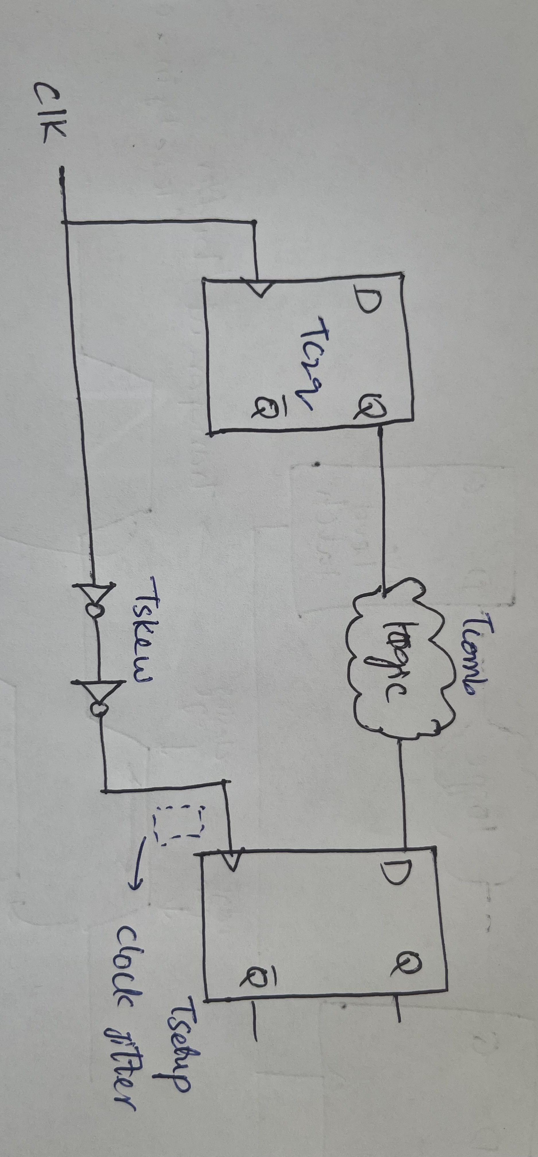
- Setup Check
Tc2q + Tcomb + Tsetup <= Tperiod
Setup check with clock skew
Tc2q + Tcomb + Tsetup <= Tperiod + Tskew
- If Tskew is +ve - addition margin
- If Tskew is -ve - pessimistic
Setup check with clock skew and jitter
Tc2q + Tcomb + Tsetup <= Tperiod + Tskew . Su
- Hold Check
Tc2q + Tcomb >= Thold
Hold check with clock skew
Tc2q + Tcomb >= Thold + Tskew
- if Tskew is +ve - hold pessimistive
- if Tskew is -ve - relax
Hold check with clock skew and jitter
Tc2q + Tcomb >= Thold + Tskew + Hu
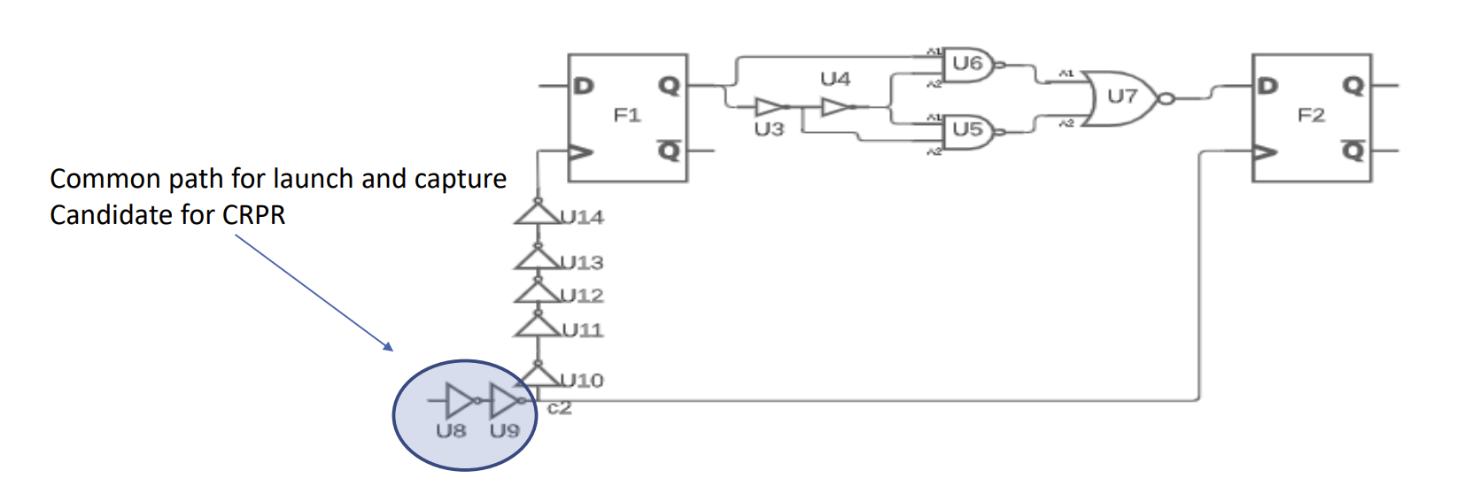
- Different delay values on paths
- for setup pessimistic - launch path (max delay) & capture path (min delay)
- for hold pessimistic - launch path (min delay) & capture path (max delay)
- for Undue pessimism -
- The situation where the timing analysis tool reports timing violations that do not actually exist in the design.
- This can occur due to various reasons such as inaccurate modeling of the design, incorrect setup of the timing constraints, or over-conservative timing margins.
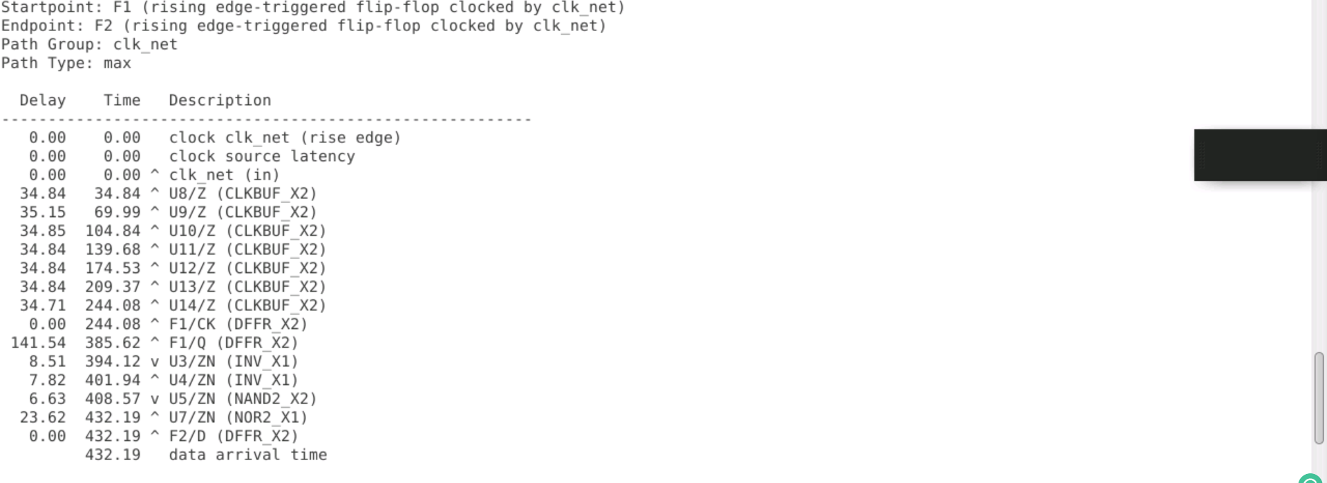
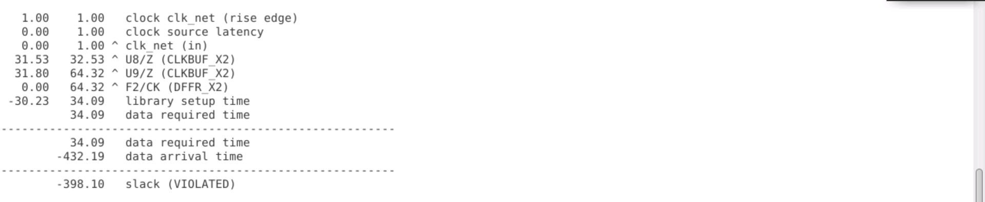
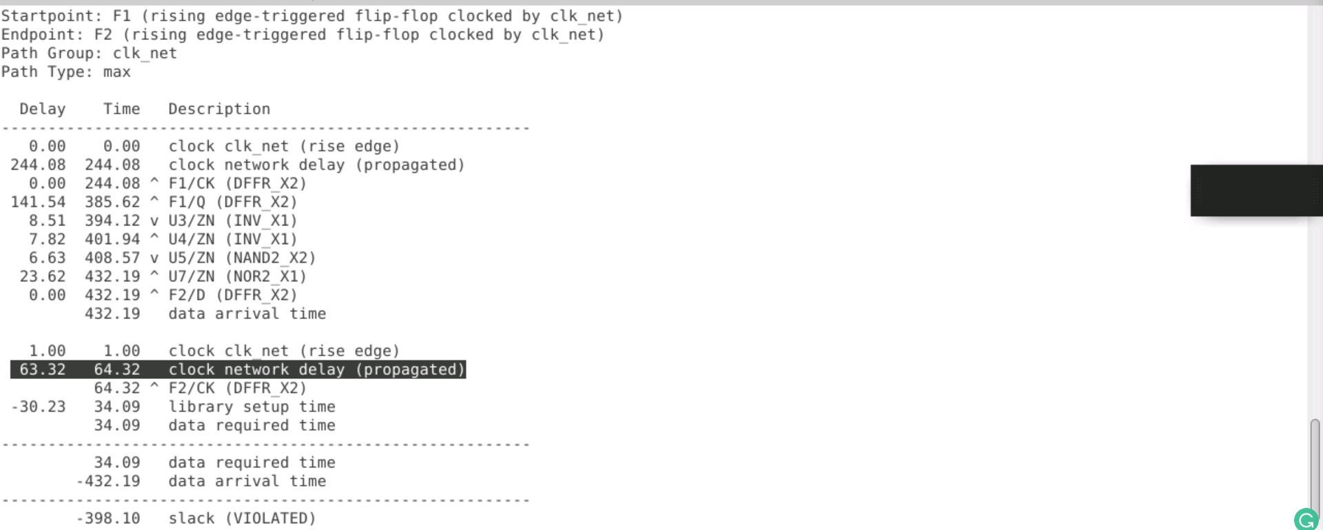
- The CPPR technique is used to reduce clock path pessimism where there is too much pessimism.
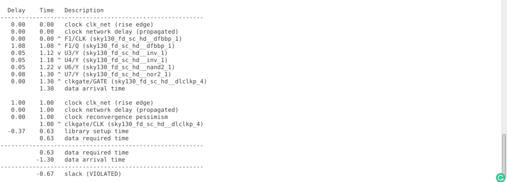
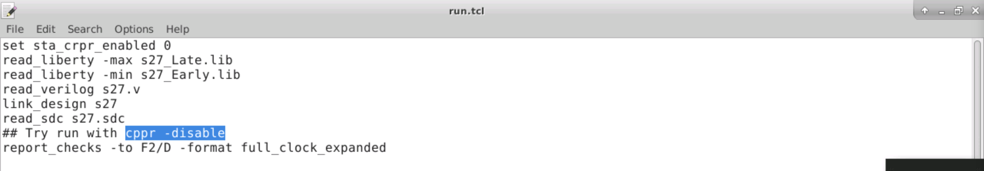
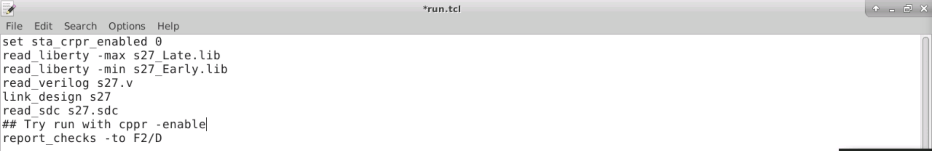
cd lab3
ls
sta run.tcl | tee out.txt
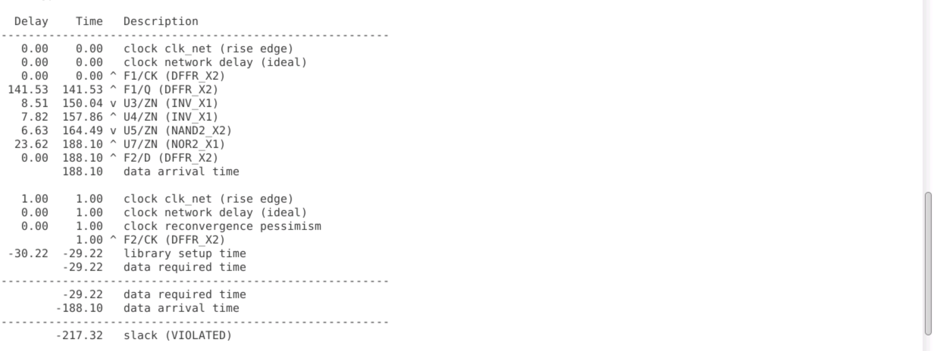
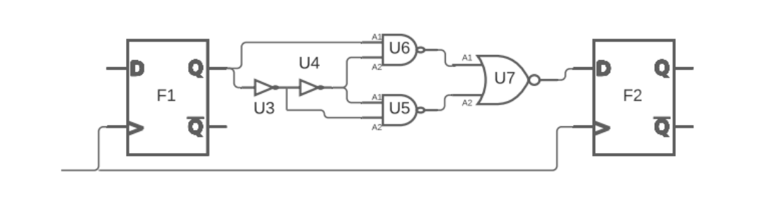
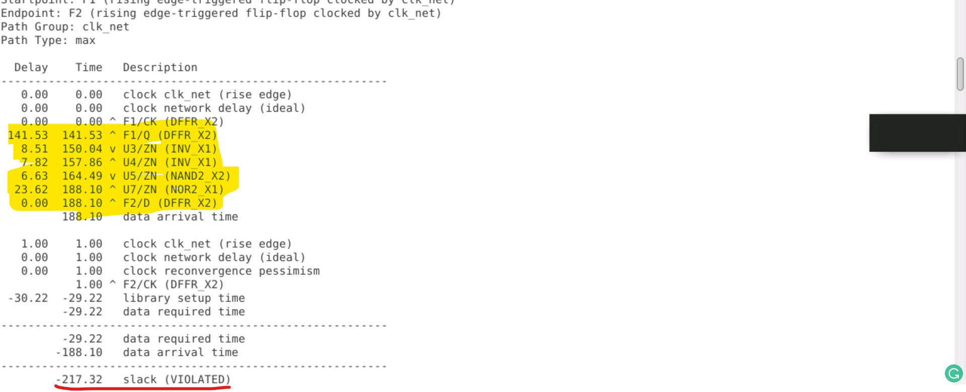
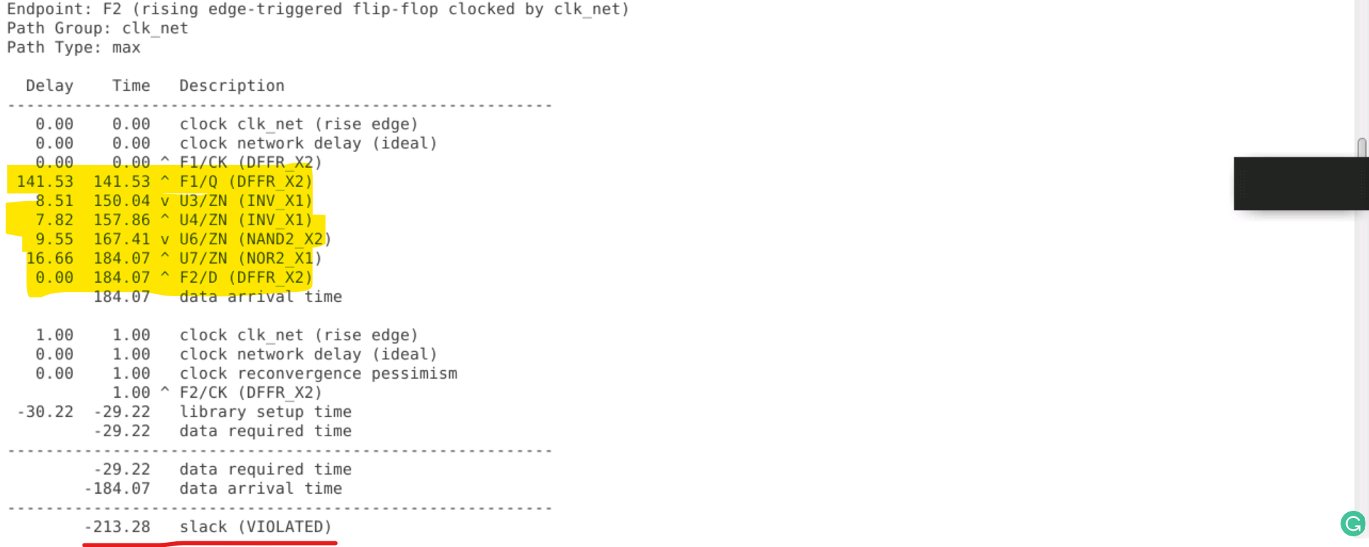
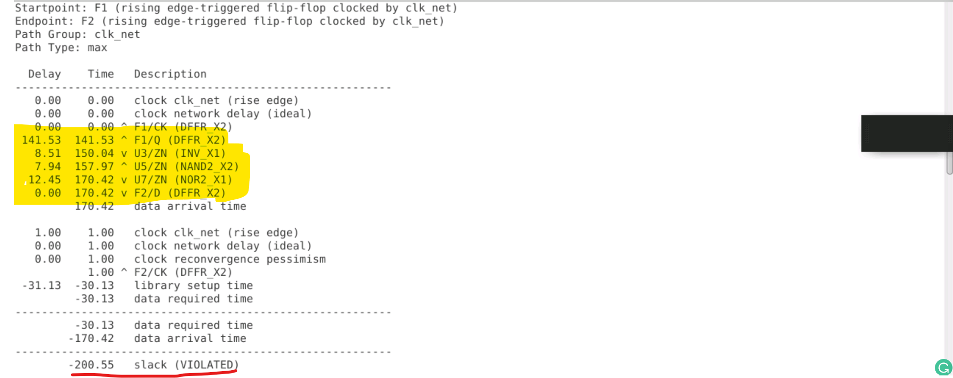
report_checks –from F1/CK -endpoint_count 100

paths
Crosstalk - The coupling capacitors can lead to delays in the signal propagation time and can affect the timing of the signals in the neighboring lines, leading to potential signal integrity issues.
- Crosstalk - Impacting Delays
- Noise can caused by coupling of switching activity of he victim with switching activity of the agressor.
- Crosstalk - glitches
- A steady signal net can have a glitch due to charge transferred by the switching.
- A signal can control the path of the clock at a cell
- The signal must be used as clock downstream
- feed a flop or latch clock pin
- feed output port
- feed generated clock
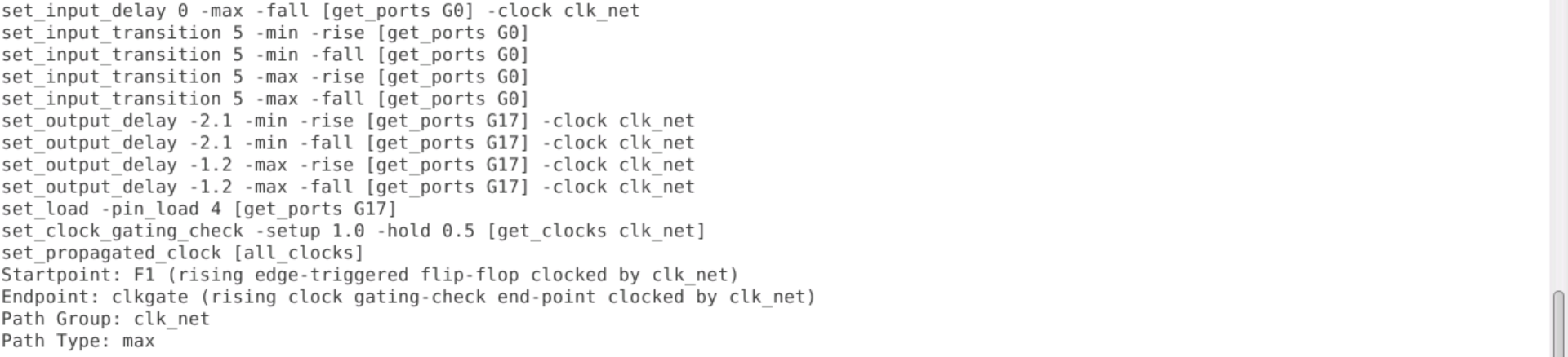
- Active high clock gating checks - occurs on
ANDandNANDcells - Active low clock gating checks - occurs on
ORandNORcells
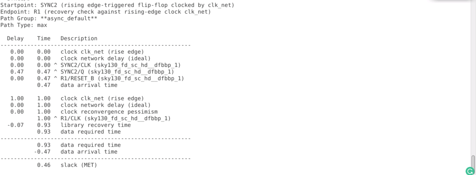
- Assertion is asynchronous event or no reation with clock
- De-assertion causes flop to become dependent on clock (Due to the unknown state, timing checks must be performed)
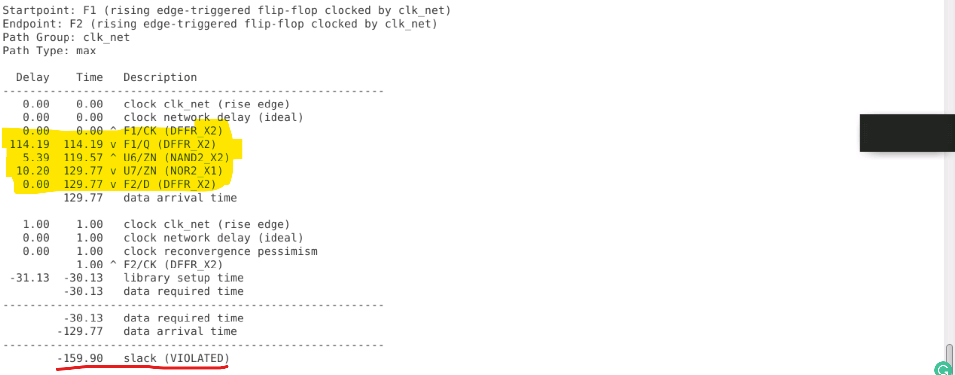
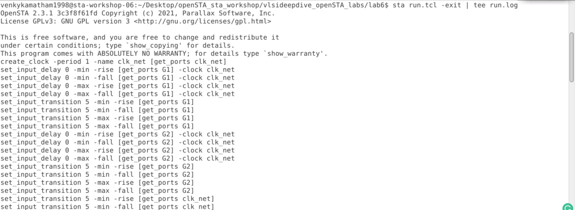
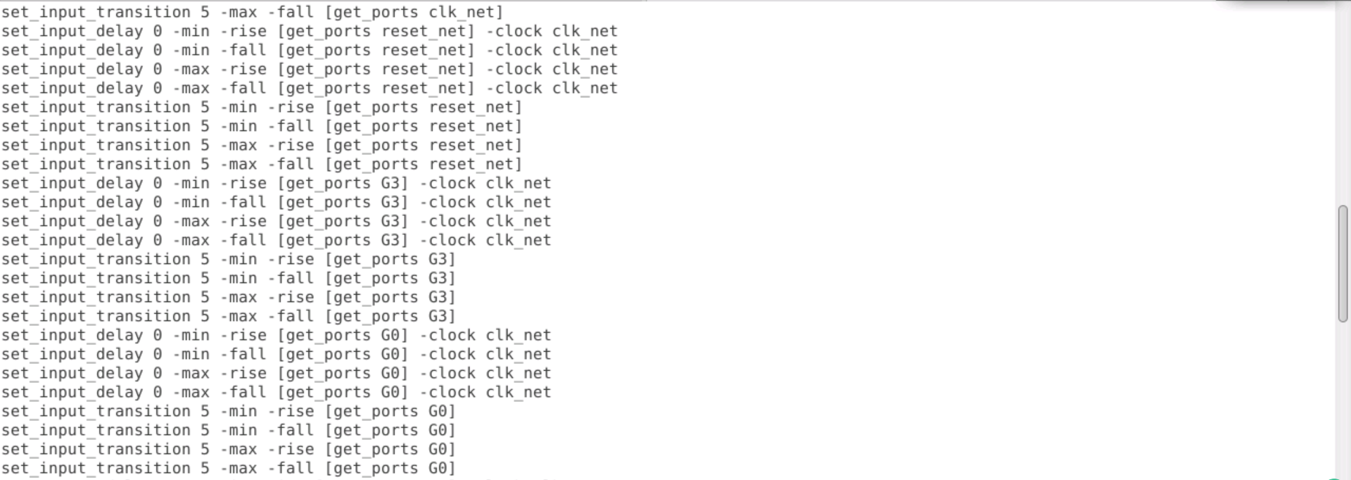
  cd lab6
  leafpad run.tcl
  sta run.tcl | tee run.log
  cd lab7
  leafpad run.tcl
  sta run.tcl | tee run.log
- Clock groups indicate whether or not a clock is synchronised and these clock groups are
- synchronous clocks - events happen at a fixed phase relation
- Asynchronous clocks - no fixed phase relation
- logically exclusive clocks - do not have any common active edge
- physically exclusive clocks - clock domains where there is no possibility of a common signal or path between them. These domains have independent clock sources and are completely isolated from each other to prevent any clock skew or crosstalk issues.
 set_clock_transition - changing 1/0 or 0/1
 set_clock_uncertainity - for clock skew and jitter
 set_clock_latency - source and network latency
 set_clock_sense - stopping the clock or specifying sense
    set_clock_sense -stop_propagation
    set_clock_sense -positive
 set_ideal_network
- Path Specification
- from - startpoint (ports/clock pins)
- to - endpoint
- through - nets/nodes
set_false_path- Don't time the pathset_multicycle_path- use to chnage the default behaviourset_max_delay- maximum delay on pathset_min_delay- minimum delay on pathset_disable_timing- disable certain timing (used for arcs)
- Multiple modes
set_case_analysis - specifies a certain portion of design and a constant value
CPPR (Clock Path Power Reduction)
- It is a technique used to reduce the power consumed by the clock network in a chip design.
- The CPPR technique involves optimizing the clock tree to reduce the overall clock skew and jitter, while also minimizing the power consumed by the clock buffers and other clock distribution elements.
- This is achieved by carefully selecting the location and size of clock buffers, as well as using other techniques such as clock gating and frequency scaling.
- The goal of CPPR is to reduce the overall power consumption of a chip design while maintaining acceptable timing and performance characteristics.
cd lab4
leafpad run.tcl

sta run.tcl | tee out.txt
ECO – Engineering Change Order
-
During the ECO cycle, we perform various analyses one by one for each check that needs to be closed but cannot be closed until the PnR stage.
-
There are specialised signoff tools that assist us in analysing the issue and recommending the changes that must be made in order to close the issue.
-
The suggested change is captured in an eco file.
cd lab5
leafpad run.tcl

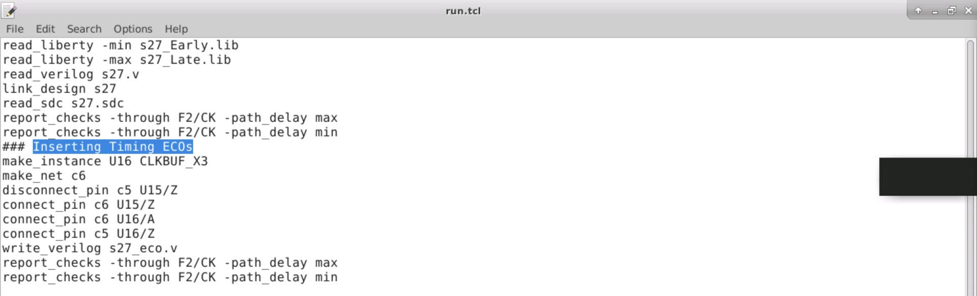
sta run.tcl | tee run.log
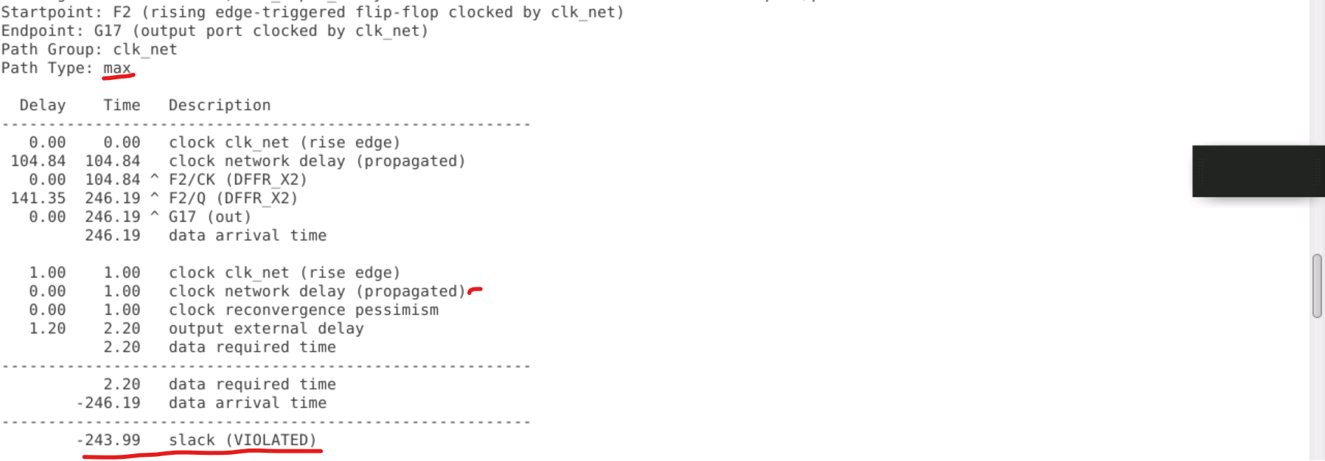
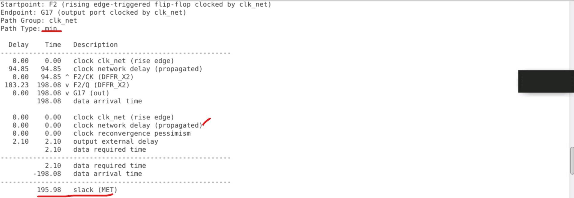
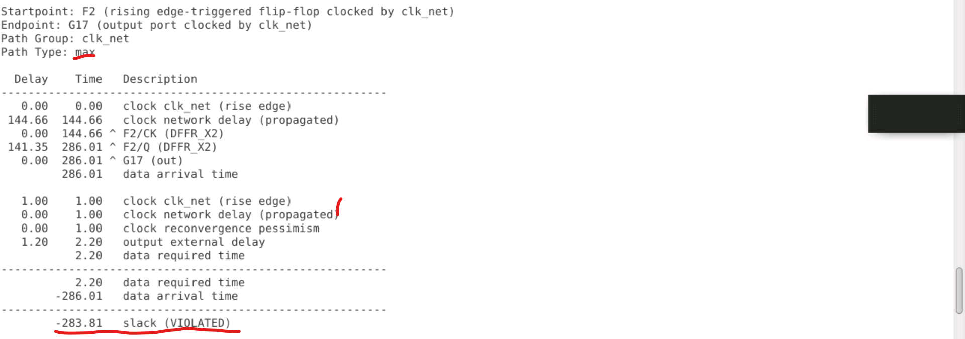
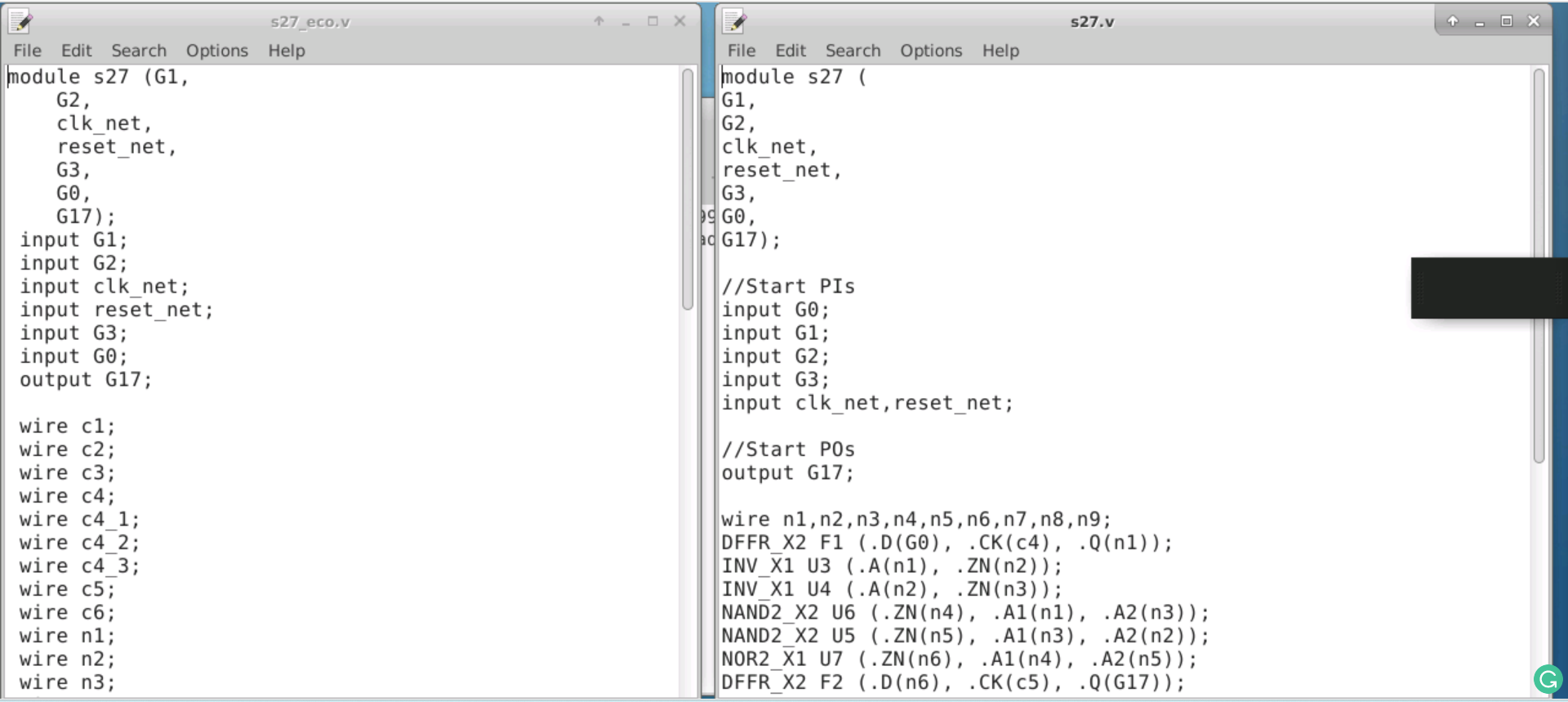
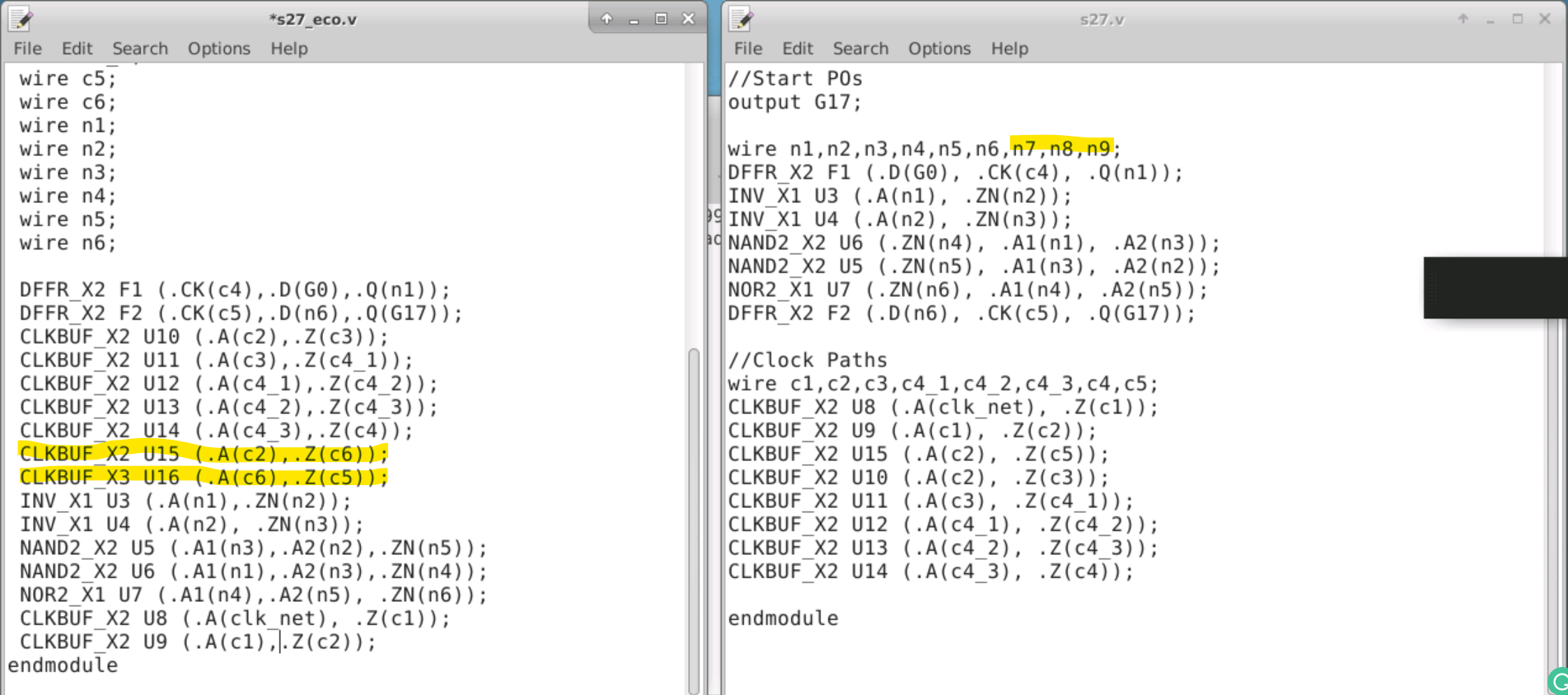
Difference between s27_eco.v and s27.v
- https://github.com/The-OpenROAD-Project/OpenSTA/blob/master/doc/OpenSTA.pdf
- https://people.eecs.berkeley.edu/~alanmi/publications/other/liberty07_03.pdf
- https://www.vlsisystemdesign.com/spef-format-part-1/
- https://www.vlsisystemdesign.com/?s=cppr
- https://www.vlsisystemdesign.com/the-beauty-of-slack-based-timing-eco/