Blog
I made some updates to the instruction set and hardware design:
- Moved the
EXCHinstruction from the core CPU implementation to the assembler- That instruction in particular required too many connections to and from
ABandAA
- That instruction in particular required too many connections to and from
- Removed the hardcoded load instructions (
LDA1,LDAF,LDB1,LDBF)- These provided minimal benefit (1 clock cycle) compared to the additonal hardware needed
- Moved the bit set and clear instructions for
AA(BCAA,BSAA) to be implemented by the assembler - Created another register (
AC) which can be used as a counter register for loops and for temporary storage. It is not connected to the ALU orAB, so minimal additional hardware is needed.- Relevant instructions were added to support the new register
The emulator has been updated with these changes.
I have added another register: AC. This register has limited functionality, and is easy to implement. It is not connected to the ALU and cannot be used for arithmetic operations. It is supported by the MOVE instructions and can be used for temporary storage. It can also be used as a counter for loop operations with the INCC instruction (INCC sets the Z flag if the result is zero).
| Mnemonic | Previous Opcode | Clocks | Side Effects | Assembler Implementation |
|---|---|---|---|---|
BCAA |
0x10 - 0x17 | 3 |
AB modified |
Load AB with bit mask, then ANDD
|
BSAA |
0x18 - 0x1F | 3 |
AB modified |
Load AB with bit mask, then ORRR
|
EXCH |
0x40 | 6 | Uses stack, AC modified |
PUSH AA, AB->AA, AA->AC, POP AA, AA->AB, AC->AA
|
| Mnemonic | Opcode | Previous opcode mnemonic |
|---|---|---|
MOVE AC->AA |
0x41 | MOVE AB->AA |
MOVE AA->AC |
0x49 | MOVE AA->AB |
XNOR |
0x5A | SHRL |
INCC |
0x63 | DECB |
LDC0 |
0x6A | N/A |
| Mnemonic | New opcode | Old opcode |
|---|---|---|
MOVE AB->AA |
0x40 | 0x41 |
MOVE AA->AB |
0x48 | 0x49 |
LDB0 |
0x69 | 0x6c |
PUSH FL |
0x31 | 0x32 |
POPP AA |
0x34 | 0x38 |
POPP FL |
0x35 | 0x39 |
Also, all shift instruction opcodes are increased by 1 (i.e., 0x5A - 0x5E are now 0x5B - 0x5F).
| Mnemonic | Opcode | Reason |
|---|---|---|
DECB |
0x63 | Limited usefulness; user register AC for loops |
LDA1 |
0x69 | Limited usefulness; only saves one clock cycle |
LDAF |
0x6B | Limited usefulness; only saves one clock cycle |
LDB1 |
0x6D | Limited usefulness; only saves one clock cycle |
LDBF |
0x6F | Limited usefulness; only saves one clock cycle |
-
SUBBandNEGA(2's complement) can be implemeted in a single clock cycle with a multiplexer-adder based ALU (74HC153 MUX, 74HC283 adder) -
INCAcan be implemented with a hardcoded 0x01 on ALU -
DECAcan be implemented with a hardcoded 0xFF on ALU -
INCBandINCCcan be implemented using counter functionality of the register;INCBdoes not affect flags -
LDA0,LDB0,LDC0can be implemented using the CLR/RST control line on the register chip
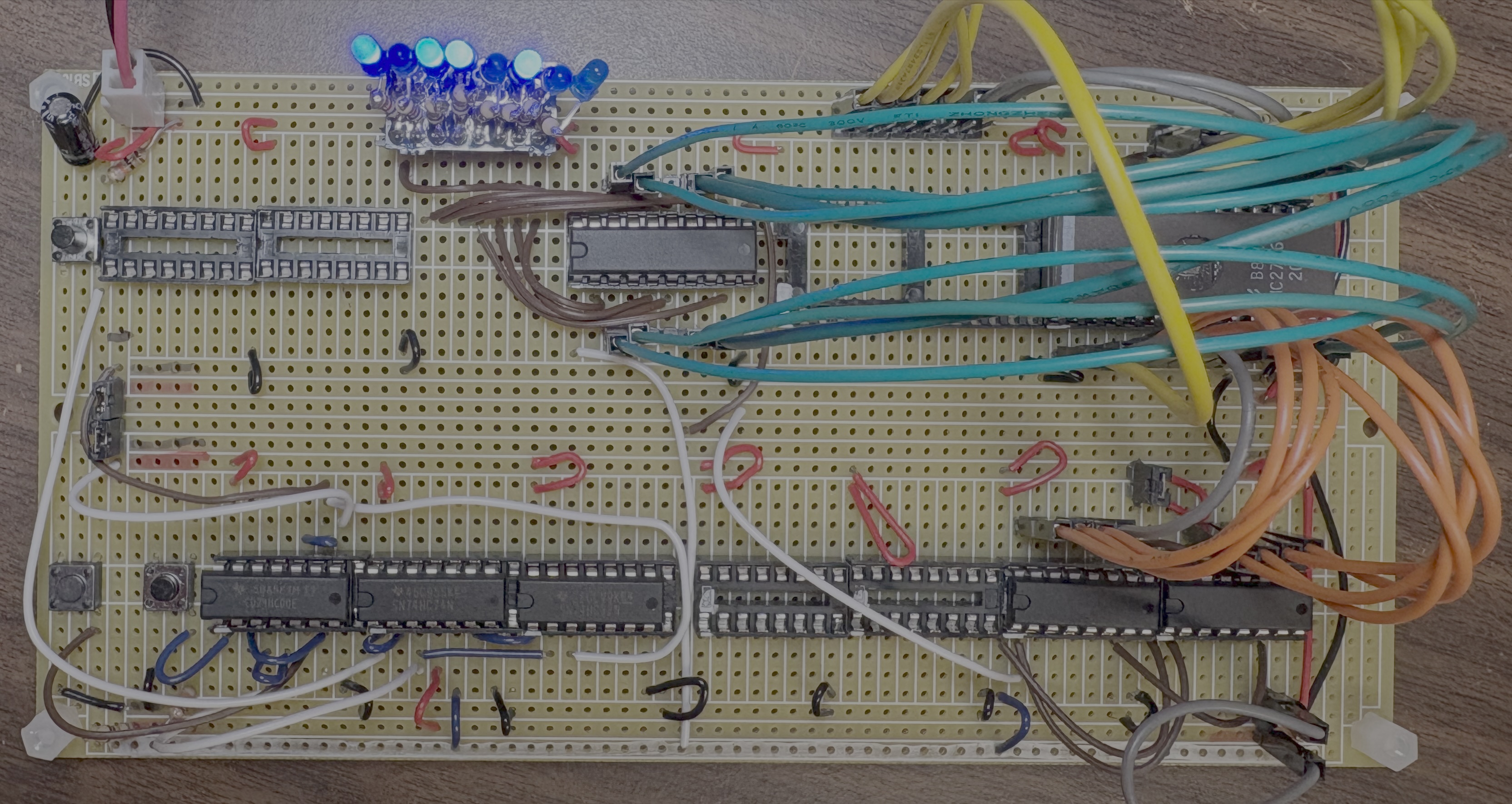
I transferred my PC and IR circuit from a solderless breadboard to a soldered breadboard. I needed breadboard space for my next circuit block implementation, and the PC/IR circuit is stable and fairly complete.
Protoboard:
Compared to the original breadboard:
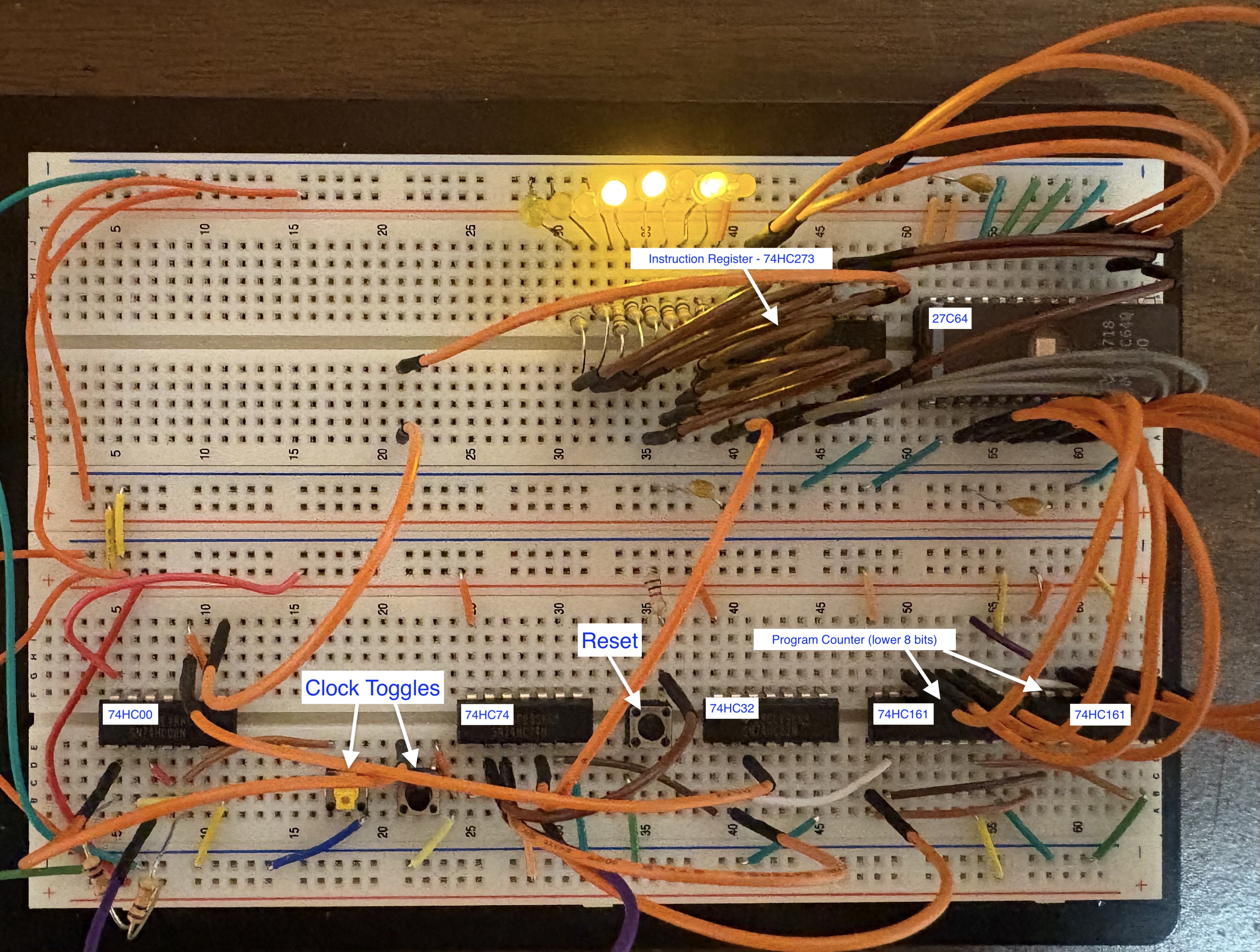
I have implemented the PC and Fetch logic in hardware: the clock increments the PC and fetches an instruction into IR with each clock cycle. PC is incremented on the rising edge of the clock, and IR latches the instruction from memory on the falling edge.
There is some additional logic to ensure that the first clock edge after coming out of reset is falling, so that the first instruction is read from memory location 0x0000:
- The external /EXT_RST signal is fed into the D and /CLR inputs of a 74HC74 DFF
- The external EXT_CLK signal is fed into the CLK inputs of the DFF
- The Q (non-inverted) output of the DFF is used as the /RST signal internal to the CPU
- The internal /RST will only go inactive after a rising edge of EXT_CLK (since it is latched by DFF)
- The /Q (inverted) output of the DFF is fed to an OR gate on a 74HC32 along with the external CLK signal, producing a CLK signal used internally by the CPU
- This CLK signal is only active when /RST is inactive (high)
- The internal CLK signal is at a constant high level when /RST is active
- By latching the reset signal and forcing CLK high during reset, then the first clock transition after reset is a falling edge
- The falling edge of CLK latches in data into
IRfrom the address of the currentPC, which is cleared to 0x0000 by reset - The rising edge of CLK then increments
PCto address 0x0001
Schematics:
Note that the Memory (EPROM in this case) is not part of the CPU, but is a necessary component of the overall system. I have it drawn on the same schematic sheet with IR for now as a convenience, but it will be split into a separate sheet in a future iteration.
I have also made a slight change to the instruction set. I re-arranged the Bit Addressing Mode opcodes so that I could free up opcode 0x00 for the NOOP instruction. It just makes the overall design simpler if 0x00 is NOOP. The emulator has been updated accordingly.
As I was working on the overall block diagram and data connections between the various components, I realized that implementing the PUSH and POPP stack operations for every register makes the internal CPU connections much more complicated than I wanted, for instructions that likely won't be used very often. The only registers now supported by PUSH and POPP are AA and FL.
I also realized that a much more useful operation would be to have a way to store AA without having to write it to memory. Since AB is not used as the result of any operations, it could be useful as a "scratch" register if you need to temporarily store the value of AA. So I added the EXCH instruction, which swaps the values in registers AA and AB. This can also be useful when pushing items to the stack: temporarily store the value of AA in AB, use AA to push/pop whatever registers you need to save, then EXCH register AA back. Opcode list and the emulator have been updated. The implementation of the EXCH instruction won't actually move the bits between the two registers, but will update the control signals so that they point to the other register.
Now that I have a pretty good idea on the design of the CPU, it's time to get started on the hardware. The first step is generating a clock signal. While the clock is not technically a part of the CPU itself, it is a key input into the system and is necessary for any testing of the hardware.
Once this design is fully realized and implemented on a PCB, it should be able to run at a clock rate of several MHz. However, until then, I will want to run it at a much lower speed for testing and debugging. I have three different clock generator circuits.
The manual clock generator makes it easy to test and verify the functionality of the circuits as I build them and can also be used for debugging where single-stepping the clock will be useful.
The manual clock circuit is just two push buttons debounced with an SR-latch implemented with two NAND gates from a 74HC00 chip and a couple pull-up resistors.

This circuit lets me manually toggle clock transitions from low-to-high and high-to-low as needed to check the circuit operation.
This setup uses an Arduino UNO and a simple sketch that lets me select a desired clock rate (from 31 Hz to 65535 Hz). This is useful for running tests that would be too cumbersome to manually toggle the clock (e.g., testing that the PC counter chips correctly cascade the output of the 4-bit counters to the next counter block). It also gives me an indication that the circuit is robust enough to move on to MHz range testing.
For clock rates in the MHz range, I plan to use a TTL Clock Oscillator. These parts integrate the resonator and oscillator components along with a buffer circuit into a single package, rather than having to deal with multiple discrete parts to create the clock signal.
Once I started working on the hardware for my original design, I quickly realized that two-byte opcodes were not going to work (or were at least going to make the hardware much more complicated than I envisioned). I needed to move to a single-byte instruction length. See the wiki pages under the "Current Design" heading for the updated design. The old design is available under the "Previous Design" heading. I have updated the emulator/disassembler to the Version 2 design.
I have completed the implementation and limited testing of an emulator and disassembler for my CPU design.
I have created and documented an initial design including register list, addressing modes, supported instructions, opcode structure and opcode list. See the wiki for details.
Starting on my homemade CPU. Created this repo and associated wiki. Getting started on the design.
- Online logic-gate schematic generator tool
- EasyEda PCB design software, pro version
- Clock circuit schematics: manual